Multi-layer overlaid storage disk with same substrate compatible with multiple interfaces, and packaging process thereof

A technology for storage disks and substrates, applied in the directions of connection, fixed connection, electrical components, etc., can solve the problems of complex USB Type-C connector mounting process, poor USB Type-C connector compatibility, and thick USB Type-C connector thickness. The circuit structure is stable, more portable and easy to carry.

Active Publication Date: 2016-12-21
SHENZHEN SHICHUANGYI ELECTRONICS +1
View PDF10 Cites 2 Cited by
  • Summary
  • Abstract
  • Description
  • Claims
  • Application Information

AI Technical Summary

Problems solved by technology

[0006] 1. The mounting process of the traditional USB Type-C connector is complex, with many assembly processes and high cost;
[0007] 2. The traditional USB Type-C connector has poor compatibility;
[0008] 3. The shielding shell of the traditional USB Type-C connector is welded by bending the hardware, which makes the thickness of the USB Type-C connector thicker, which cannot meet the user's pursuit of smaller and ultra-thin requirements
Traditionally, the signals applied to the stack of memory disk chips flow through wires. Long wires will cause signal delay and occupy more space, resulting in the production of large memory disk chip stacks.

Method used


Image

  • Multi-layer overlaid storage disk with same substrate compatible with multiple interfaces, and packaging process thereof
  • Multi-layer overlaid storage disk with same substrate compatible with multiple interfaces, and packaging process thereof
  • Multi-layer overlaid storage disk with same substrate compatible with multiple interfaces, and packaging process thereof

Examples


Embodiment Construction

[0058] The preferred embodiments of the present invention will be described in detail below in conjunction with the accompanying drawings, so that the advantages and features of the present invention can be more easily understood by those skilled in the art, so as to define the protection scope of the present invention more clearly.

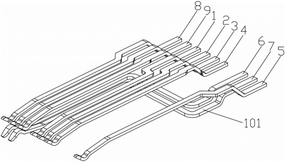
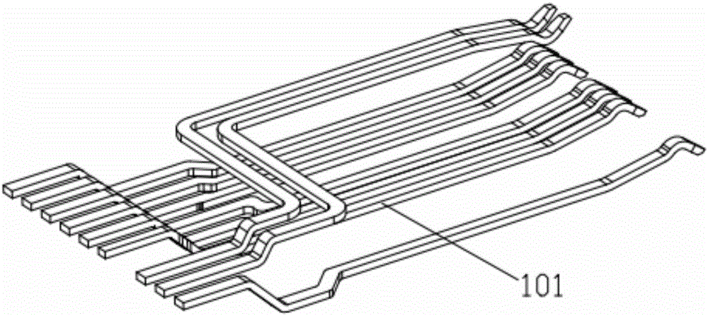
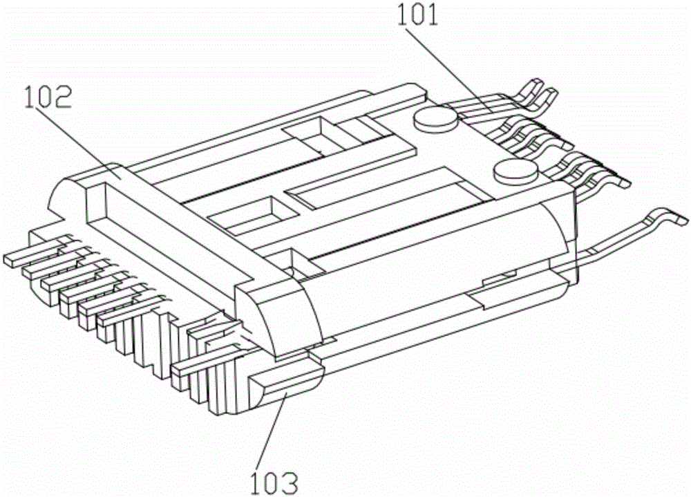
[0059] Please refer to the attached Figure 1~12 , a multi-layer stacked storage disk compatible with multiple interfaces with the same substrate of the present invention, the storage disk includes a TypeC high-speed male head, a package connected to the TypeC high-speed male head, and a stacked storage disk placed inside the package; The TypeC high-speed male head includes a 9-pin terminal 101, a solder pad, an upper cover 102, and a lower cover 103. A terminal slot is provided on the joint surface of the upper cover 102 and the lower cover 103, and the terminal 101 is fixed in the terminal slot. Inside, the pad is a 10pin pad, and the pad is pr...


PUM

PropertyMeasurementUnit
Lengthaaaaaaaaaa

Abstract

The present invention discloses a multi-layer overlaid storage disk with the same substrate compatible with multiple interfaces. According to the storage disk, an interface of the storage disk is replaced with a TypeC high-speed male connector interface, and a packaging structure is changed. A memory, and a processing chip and an electronic element are disposed at an upper layer and a lower layer, so that the whole storage disk is reduced in structure width, and is convenient to carry. Packaging glue is used for filling twice, so that the interior circuit structure is more stable. Wafer layers are of a ladder type and are overlaid, so that a connecting distance between edge connectors is shortened, signal loss is reduced, and the cost is saved. The storage disk has a small structure and is easy to carry. Due to the detection resistor 10-PIN substrate comprising TypeC, the substrate of a fixed resistor is compatible with a USB, a 9-pin male connector, a MicroUSB, an OTG, a TypeC, an iphone connector, a Lighting adapter and so on. The multi-layer overlaid storage disk is compatible with the USB, 9-pin male connector, TypeC, MicroUSB, OTG, and iphone Lighting male connector mounting.

Description

technical field [0001] The invention relates to the technical field of storage disks, in particular to a multi-layer stacked storage disk compatible with multiple interfaces with a substrate and its packaging process. Background technique [0002] With the gradual popularization of electronic products, the manufacturing technology of the memory card used with the product not only has a large increase in storage capacity, but also has a significant improvement in practicality. The card itself provides better compatibility. Make it more convenient for consumers to use in practice. [0003] The storage disk is suitable for a standard USB interface, and the storage disk is provided with a USB gold finger that can be electrically connected to the standard USB interface. In order to protect the USB golden finger, a general storage disk is usually provided with a casing and an outer cover of the sealed casing, and the outer cover can accommodate the USB golden finger therein. Whe...

Claims


Application Information

Patent Timeline
IPC IPC(8): H01L25/16H01L21/60H01R12/57
CPCH01L24/13H01L24/48H01L24/85H01L25/16H01R12/57H01L2224/13023H01L2224/13013H01L2224/13015H01L2224/48229H01L2224/48091H01L2224/48145H01L2924/00014H01L2924/00012
Inventor 倪黄忠何霞
Owner SHENZHEN SHICHUANGYI ELECTRONICS
Why Eureka
Try Eureka