PCB and PCBA

A groove bottom and solder paste technology, which is applied to printed circuits, printed circuits connected with non-printed electrical components, electrical components, etc., can solve problems such as virtual soldering, large amount of solder paste 4', and poor control of the amount , to achieve the effect of ensuring the overall structural strength, improving heat dissipation efficiency, and increasing installation space

Inactive Publication Date: 2018-08-10
DONGGUAN SHENGYI ELECTRONICS
View PDF8 Cites 1 Cited by
  • Summary
  • Abstract
  • Description
  • Claims
  • Application Information

AI Technical Summary

Problems solved by technology

Generally speaking, such a structure has the following disadvantages: since the depth control of the metallization groove has a certain tolerance, and the distance from the pad to the groove wall is usually relatively short, in the process of fixing the component 5', the solder paste 4 The amount of 'is not easy to control. A small amount of solder paste 4' will lead to

Method used


Image

  • PCB and PCBA
  • PCB and PCBA
  • PCB and PCBA

Examples


Example Embodiment

[0040] Example one

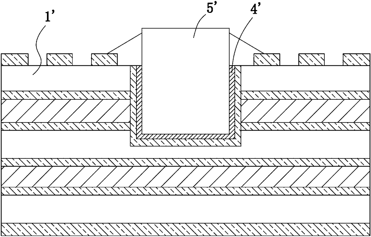
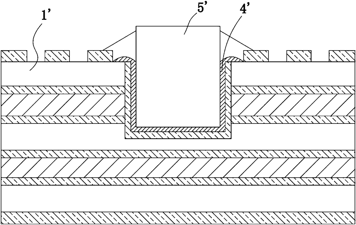
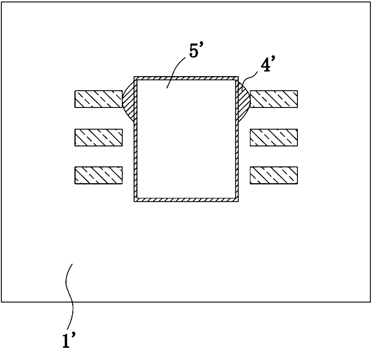
[0041] This embodiment provides a PCB 1, which includes a first groove 2 and a second groove 3. The first groove 2 is a non-metallized groove, which is opened on one side of the PCB 1, and the second groove 3 It is opened in the groove bottom of the first groove 2, the groove bottom and the groove wall of the second groove 3 are metalized, and the second groove 3 is provided with a solder paste 4.

[0042] In this embodiment, the PCB 1 is formed by pressing three core boards, but the number is not limited to this. For example, it may also be formed by pressing multiple core boards such as two or four. Before pressing, at least one prepreg is laminated between two adjacent core boards, and the number of prepregs is selected according to the actual pressing situation.

[0043] This embodiment also provides a PCBA (Printed Circuit Board+Assembly), such as Figure 4-Figure 6 As shown, the PCBA includes a component 5 and the PCB 1 provided in this embodiment. The co...

Example Embodiment

[0068] Example two

[0069] This embodiment provides a PCB 1. This embodiment is basically the same as the first embodiment. For brevity, only the difference between this embodiment and the first embodiment will be described. The structure of the first groove 2 in this embodiment is different from the first embodiment.

[0070] Such as Figure 7 As shown, the first groove 2 includes a middle groove 21 and a number of epitaxial grooves 22, the second groove 3 is opened at the bottom of the middle groove 21, and the horizontal cross-sectional area of ​​the second groove 3 is smaller than that of the middle groove 21 A number of epitaxial grooves 22 are arranged around the intermediate groove 21 at intervals and are all connected to the intermediate groove 21. The opening position of the epitaxial grooves 22 is selected according to the distribution of the circuit pattern on the surface of the PCB 1. Specifically, the epitaxial grooves 22 avoid The circuit pattern is arranged, so the...


PUM


Abstract

The invention relates to the technical field of PCB structures, particularly to a PCB and a PCBA. The PCB includes a first concave which is arranged at one side of the PCB and is a non-metalized groove; and a second groove arranged at the bottom of the first groove, the bottom and a wall of the second groove being metalized, and solder paste being arranged in the second groove. The PCBA includes components and the abovementioned PCB, the components are welded in the second groove through solder paste, the solder paste is not higher than a substrate at an opening of the first groove. The non-metalized first groove is arranged in the PCB, thereby providing accommodating space for a small amount of redundant solder paste; a non-metalized groove wall of the first groove can effectively preventa short circuit phenomenon caused by a circumstance that the solder paste is too fast in climbing speed and is easy to spill to a surface layer of the PCB and is connected with circuit patterns of the surface layer; the bottom of the second groove is metalized, surface mounting of the components is facilitated, and heat dissipation efficiency of the components is improved; and the wall of the second groove is metalized, and electric conduction of two layers or multiple layers of circuit patterns inside the PCB can be realized.

Description

technical field [0001] The invention relates to the technical field of PCB structures, in particular to a PCB and a PCBA. Background technique [0002] Printed circuit board (PCB for short) is the provider of electrical connection for electronic components. Before the appearance of printed circuit boards, the interconnection between electronic components relied on the direct connection of wires to form a complete circuit. In contemporary times, circuit panels only exist as effective experimental tools, and printed circuit boards have occupied an absolute dominant position in the electronics industry. [0003] With the development of electronic product technology, in order to save space, the components on the PCB have been developed from surface mount to embedded mount. For embedded placement of certain components, it is required that the circuit patterns of two layers in the mounting area are disconnected (different networks), while the circuit patterns of certain two laye...

Claims


Application Information

Patent Timeline
IPC IPC(8): H05K1/02H05K1/18H05K3/34
CPCH05K1/0204H05K1/183H05K3/3478H05K2201/09036
Inventor 肖璐纪成光杜红兵孙梁傅宝林刘梦茹
Owner DONGGUAN SHENGYI ELECTRONICS
Why Eureka
Try Eureka