Through hole filling fusion HDI processing technology

A processing technology and board body technology, applied in the field of through-hole filling and HDI processing technology, can solve problems such as cracks, uneven copper block and PCB handover position, and inability to process HDI products, etc., to achieve simple processing flow and convenient placement Effect

Active Publication Date: 2020-06-12
SUZHOU LANGCHAO INTELLIGENT TECH CO LTD
View PDF9 Cites 1 Cited by
  • Summary
  • Abstract
  • Description
  • Claims
  • Application Information

AI Technical Summary

Problems solved by technology

Due to the existence of processing errors, the distance between the lower side of the uppermost inner core board core and the upper side of the lowermost inner core board core will be inconsistent with the height of the copper block, so the copper block and PCB handover position will exist. The problem of unevenness, when mounting electronic components, it is easy to cause problems such as poor placement of components
[0008] 2. When inserting metal copper blocks, slots need to be opened, and the slots need to be slightly larger than the copper blocks. Since the insulating PP has a certain fluidity after

Method used


Image

  • Through hole filling fusion HDI processing technology
  • Through hole filling fusion HDI processing technology
  • Through hole filling fusion HDI processing technology

Examples


Embodiment 1

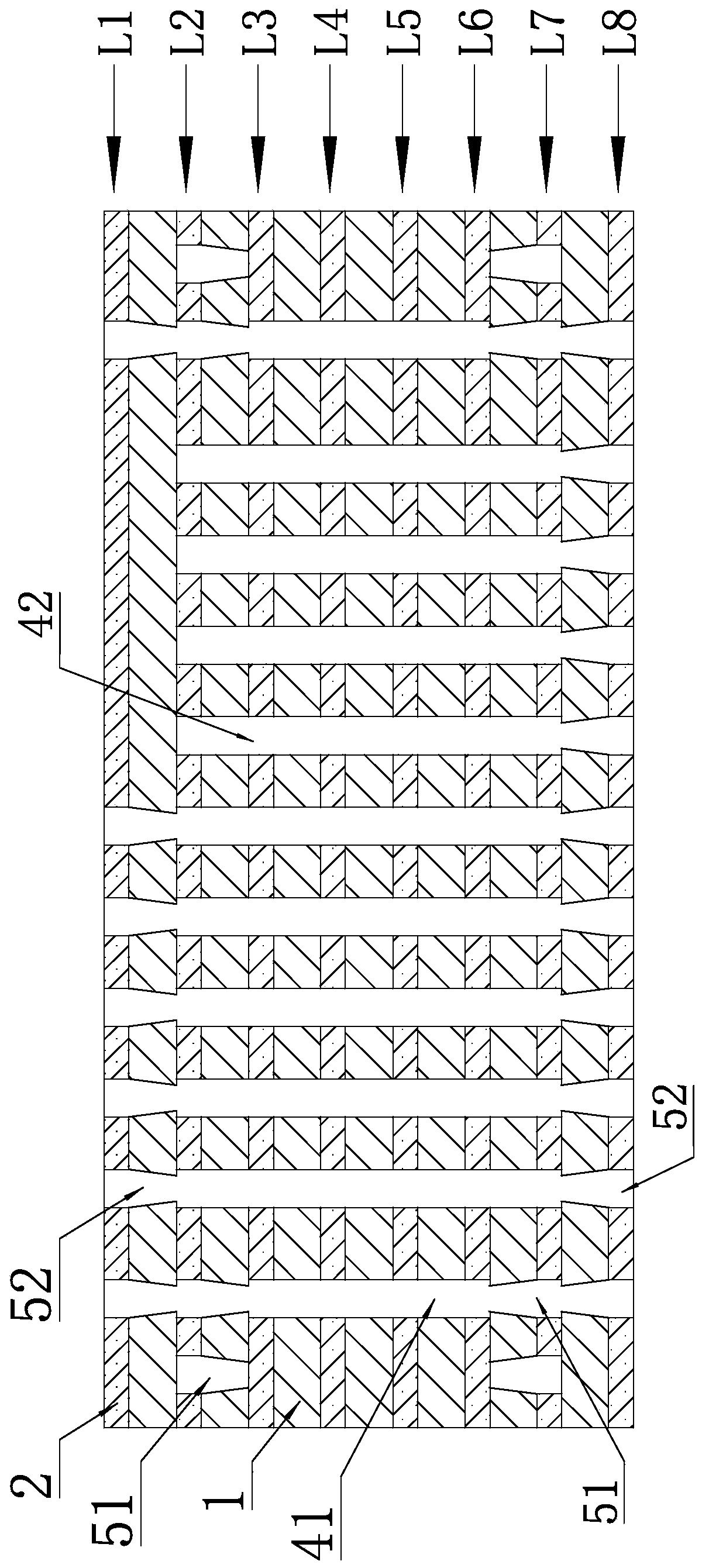
[0060] Such as figure 1 As shown, first, according to the length of the through holes, the through holes are sorted in ascending order, and the first through hole 41 and the second through hole 42 are named in sequence.

[0061] Second, the copper foil layer 2 where the first through hole 41 is located is the third layer ( L3 ), the fourth layer ( L4 ), the fifth layer ( L5 ) and the sixth layer ( L6 ).

[0062] Thirdly, the copper foil of the third layer (L3), the fourth layer (L4), the fifth layer (L5) and the sixth layer (L6) is laminated to obtain the first plate body.

[0063] As a specific implementation manner, the first board described in this embodiment is formed by laminating two layers of inner core boards through insulating PP.

[0064] Fourth, since there is no laser hole on the first plate, only the first through hole 41 exists, therefore, according to the design requirements, the first plate is drilled to obtain the first through hole 41, and then the electrop...

Embodiment 2

[0073] Such as image 3 As shown, first, according to the length of the through holes, the through holes are sorted in ascending order, and the first through hole 41 and the second through hole 42 are named in sequence.

[0074] Second, the copper foil layer 2 where the first through hole 41 is located is the third layer ( L3 ), the fourth layer ( L4 ), the fifth layer ( L5 ) and the sixth layer ( L6 ).

[0075] Thirdly, the copper foil of the third layer (L3), the fourth layer (L4), the fifth layer (L5) and the sixth layer (L6) is laminated to obtain the first plate body.

[0076] As a specific implementation manner, the first board described in this embodiment is formed by laminating two layers of inner core boards through insulating PP.

[0077] Fourth, since there is no laser hole on the first plate, only the first through hole 41 exists, therefore, according to the design requirements, the first plate is drilled to obtain the first through hole 41, and then the electropl...


PUM

PropertyMeasurementUnit
Thicknessaaaaaaaaaa

Abstract

The invention discloses a through hole filling fusion HDI processing process, and relates to the technical field of computer hardware equipment. According to the process, a hole is drilled in a PCB, and a copper base used for heat dissipation is embedded into the PCB in an electroplating hole filling mode. The embedded copper fusion HDI technology is adopted, the surface of the position, where thecomponent needs to be mounted, of the PCB is smooth, and the problems that in the embedded technology, the height difference exists between the surface of the copper block and the surface of the PCB,the concave problem exists in the joint position of the copper block and the PCB, and when the electronic component is mounted, poor placement of the component is likely to happen are solved. Besides, the process adopts an embedded copper fusion HDI technology, the processing flow is simple, the problems of delamination, cracks and the like caused by the fact that recesses exist at the connectionpositions of the copper blocks and the PCB after metal base lamination and no base material copper exists at the connection positions of the copper blocks and the PCB in an embedded metal base technology are avoided, and HDI products with two or more orders can be processed.

Description

technical field [0001] The invention relates to the technical field of computer hardware equipment, in particular to a through hole filling fusion HDI processing technology produced by applying PCB boards. Background technique [0002] In order to facilitate the understanding of the technical background of this patent, the structure of the PCB board is briefly described first. The PCB board is a multi-layer board composed of multiple layers of copper foil layers, and an insulating layer is provided between adjacent copper foil layers. When in use, the integration of circuits is realized by conducting different layers of copper foil layers. According to the manufacturing method of PCB, it can be divided into Foil stacking method and Book stacking method. [0003] like Figure 7 As shown, the Book stacking method is to press the multi-layer inner core boards (core) together through insulating PP, and insulating PP is arranged between adjacent inner layer core boards. Here, th...

Claims


Application Information

Patent Timeline
IPC IPC(8): H05K3/42H05K3/46
CPCH05K3/42H05K3/423H05K3/424H05K3/46
Inventor 张永甲宋玉娜
Owner SUZHOU LANGCHAO INTELLIGENT TECH CO LTD
Why Eureka
Try Eureka