

PCB and PCBA
A ring groove and solder paste technology, which is applied to printed circuits, printed circuits connected with non-printed electrical components, electrical components, etc., can solve problems such as poor soldering, large amount of solder paste 4', and poor control of the amount , to achieve electrical conduction, improve heat dissipation efficiency, and facilitate placement
- Summary
- Abstract
- Description
- Claims
- Application Information
AI Technical Summary
Problems solved by technology
Method used
Image

Examples
Embodiment 1
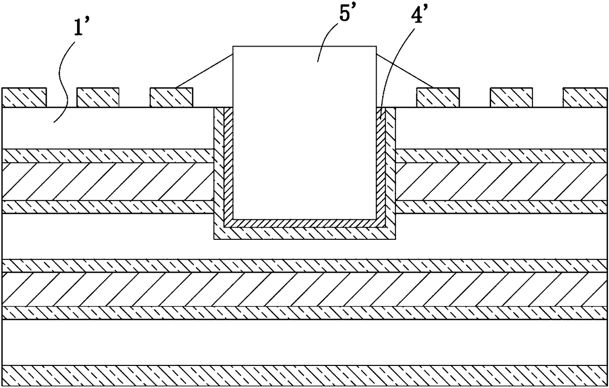
[0045] This embodiment provides a PCB 1, including a first groove 2 and a second groove 3, wherein the first groove 2 is set on one side of the PCB 1, and the groove bottom and the groove wall of the first groove 2 are metallized , the first groove 2 is provided with solder paste 4, the second groove 3 is a non-metallized groove, which is arranged at intervals around the first groove 2, and the notch of the first groove 2 and the groove of the second groove 3 There is no line graph between ports.
[0046] In this embodiment, the PCB 1 is formed by pressing three core boards, but the number is not limited thereto, for example, two or four core boards may also be formed by pressing together. Before pressing, at least one prepreg is stacked between two adjacent core boards, and the number of prepregs is selected according to the actual pressing situation.
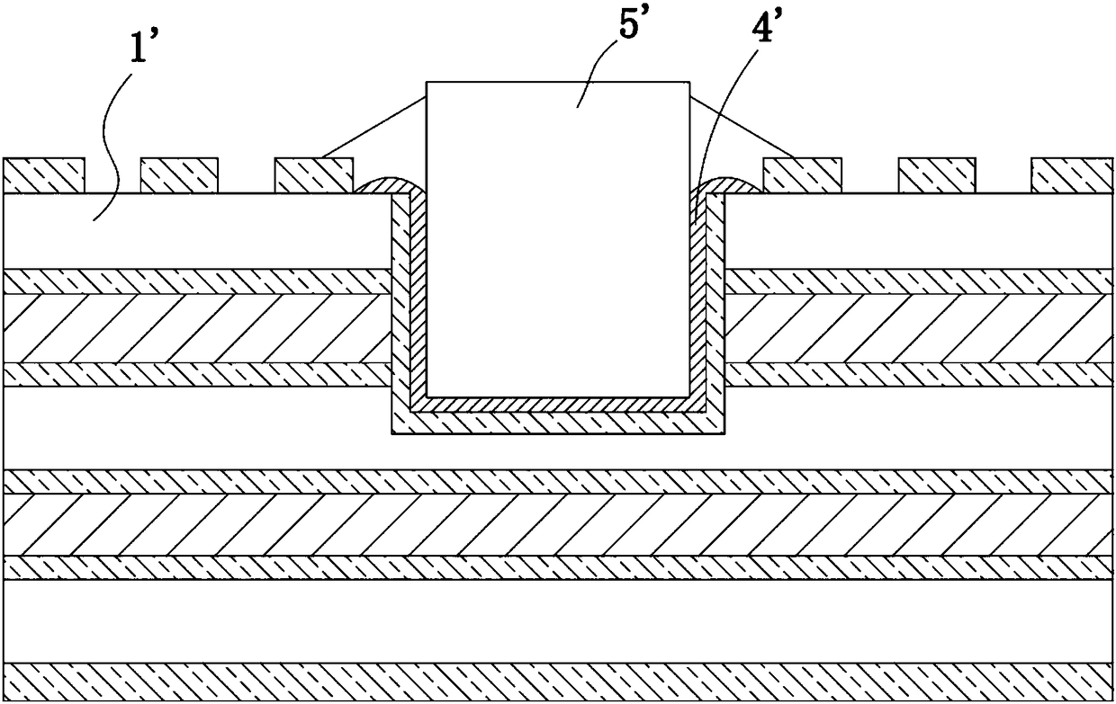
[0047] This embodiment also provides a PCBA (Printed Circuit Board+Assembly), such as Figure 4As shown, the PCBA includes...
Embodiment 2
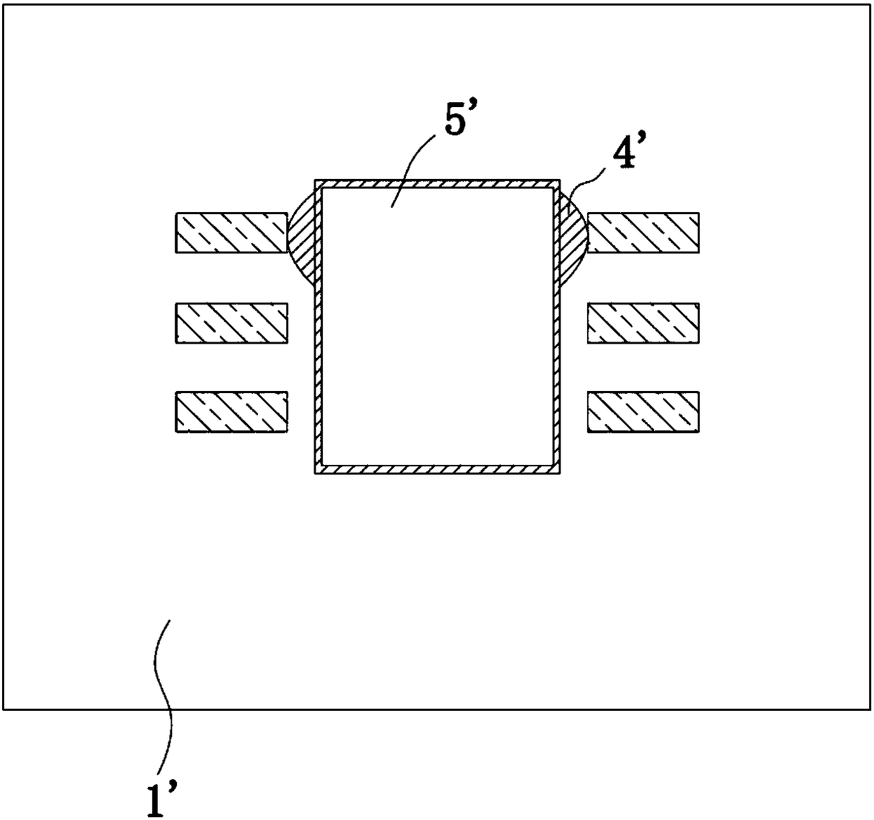
[0073] This embodiment provides a PCB 1 , which is basically the same as the first embodiment, and for the sake of brevity, only the differences between this embodiment and the first embodiment will be described. The structure of the second groove 3 in this embodiment is different from the first embodiment.
[0074] Such as Figure 8 As shown, the second groove 3 includes an annular groove 31 and several extension grooves 32. The annular groove 31 is set on the outer periphery of the first groove 2 and does not communicate with the first groove 2. Several extension grooves 32 are arranged at intervals in the annular groove 31. and are all connected to the annular groove 31, the opening position of the extension groove 32 is selected according to the distribution of the circuit pattern on the surface of the PCB 1, specifically, the extension groove 32 avoids the setting of the circuit pattern, so the length of the extension groove 32 and The width can be designed according to ...
PUM
 Abstract
Description
Claims
Application Information