Array substrate, display panel and driving method thereof and display device

An array substrate and display panel technology, applied in static indicators, optics, instruments, etc., can solve the problems of inconsistent touch signal strength, decreased touch sensitivity, and increased driving power consumption, so as to improve touch sensitivity and reduce driving. Power consumption, effect of reducing resistance

Pending Publication Date: 2017-01-04
XIAMEN TIANMA MICRO ELECTRONICS +1
View PDF11 Cites 6 Cited by
  • Summary
  • Abstract
  • Description
  • Claims
  • Application Information

AI Technical Summary

Problems solved by technology

Usually the driving circuit is arranged at one end of the data line in its extending direction, and the strip electrode has a higher resistance value, and the touch reference signal is transmitted from the end of the strip electrode closer to the driving circuit to the end farther away from the driving circuit. During the process of one end, signal attenuation will occur; the touch sensing signal will also undergo signal attenuation during the process of transmitting from the end of the strip electrode farther away from the driving circuit to the end closer to the driving circuit, which will cause the strip electrode to be close to the driving circuit. Inconsistencies in the touch signal strength between the end and the remote end, resulting in a decrease in touch sensitivity and an increase in drive power consumption

Method used


Image

  • Array substrate, display panel and driving method thereof and display device
  • Array substrate, display panel and driving method thereof and display device
  • Array substrate, display panel and driving method thereof and display device

Examples


Embodiment Construction

[0018] The application will be further described in detail below in conjunction with the accompanying drawings and embodiments. It should be understood that the specific embodiments described here are only used to explain related inventions, rather than to limit the invention. It should also be noted that, for the convenience of description, only the parts related to the related invention are shown in the drawings.

[0019] It should be noted that, in the case of no conflict, the embodiments in the present application and the features in the embodiments can be combined with each other. The present application will be described in detail below with reference to the accompanying drawings and embodiments.

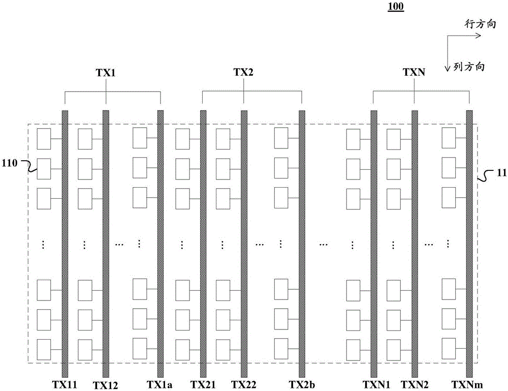
[0020] Please refer to figure 1 , which shows a schematic structural view of an embodiment of an array substrate according to the present application.

[0021] like figure 1 As shown, the array substrate 100 includes sub-pixels 110 arranged in an array along the row direct...


PUM


Abstract

The invention discloses an array substrate, a display panel and a driving method thereof and a display device. According to one embodiment, the array substrate comprises sub-pixels arranged in an array in the row direction and the column direction and multiple touch electrodes arranged in the row direction; each touch electrode comprises multiple touch sub-electrodes arranged sequentially in the row direction, and each touch sub-electrode provides a data signal to one column of sub-pixels at the display stage; each touch sub-electrode receives a touch detection signal at the touch detection stage. According to the embodiment, the touch sub-electrodes are reused as data lines, therefore, losses of touch signals in the transmission process in the touch electrodes can be effectively reduced, the touch sensitivity of a display screen is improved, and meanwhile driving power consumption can be lowered.

Description

technical field [0001] The present application relates to the field of display technology, in particular to an array substrate, a display panel, a driving method thereof, and a display device. Background technique [0002] Touch screens can be classified into self-capacitive touch screens and mutual-capacity touch screens according to their touch detection principles. In one structure of the mutual capacitive touch display screen, strip electrodes extending along the direction of the data lines are arranged on the array substrate as touch reference electrodes or touch sensing electrodes. When performing touch detection, the drive circuit is connected to the strip electrodes at one end of the strip electrodes, and provides touch reference signals to the strip electrodes or receives touch sensing signals. Usually the driving circuit is arranged at one end of the data line in its extending direction, and the strip electrode has a higher resistance value, and the touch referenc...

Claims


Application Information

Patent Timeline
Patent Type & Authority Applications(China)
IPC IPC(8): G06F3/041G02F1/133G02F1/1333G02F1/1343
CPCG02F1/13306G02F1/13338G02F1/134309G06F3/041G06F3/0414G09G3/36G06F3/0412G06F2203/04105G02F1/134336G02F1/136286G06F3/0446G06F3/0445G06F3/04184G02F1/134345
Inventor 孙莹许育民詹小静杨文强
Owner XIAMEN TIANMA MICRO ELECTRONICS
Why Eureka
Try Eureka