Display panel and display device

A technology for display panels and substrate substrates, applied in static indicators, instruments, light guides, etc., can solve the problems of poor dye filtering effect, reduced liquid crystal response time, low transmittance of display devices, etc., to improve the response time. , the effect of improving the transmittance

Active Publication Date: 2017-01-11
BOE TECH GRP CO LTD
View PDF8 Cites 40 Cited by
  • Summary
  • Abstract
  • Description
  • Claims
  • Application Information

AI Technical Summary

Problems solved by technology

[0004] The use of polarizers in the display panels of liquid crystal display devices in the prior art will lead to very low transmittance of the liquid crystal display device (for example, the transmittance is about 7%) and the thickness of the liquid crystal cell is relatively large (for example, 3um-5um) , and a larger cell thickness will reduce the response time of the liquid crystal; in the prior art, due to the poor light filtering effect of the dye itself, the color color resist made of the resin mixed with the dye will cause the low transmittance of the liquid crystal display device

Method used


Image

  • Display panel and display device
  • Display panel and display device
  • Display panel and display device

Examples


Embodiment Construction

[0034] In order for those skilled in the art to better understand the technical solution of the present invention, the display panel and the display device provided by the present invention will be described in detail below with reference to the accompanying drawings.

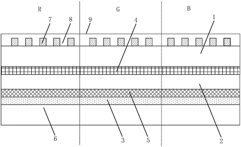
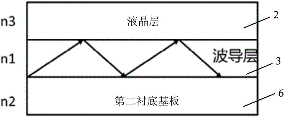
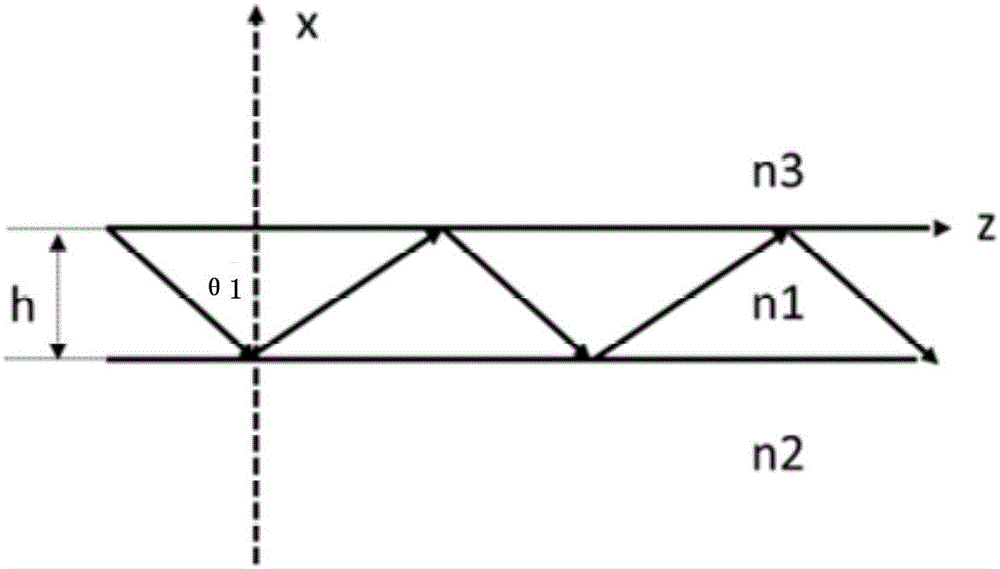
[0035] figure 1 A schematic structural diagram of a display panel provided in Embodiment 1 of the present invention, as shown in figure 1 As shown, the display panel includes a first base substrate 1, a liquid crystal layer 2, a waveguide layer 3, a grating layer, a first electrode 4 and a second electrode 5, and the liquid crystal layer 2, the first electrode 4 and the second electrode 5 are located in the waveguide Between layer 3 and the first base substrate 1. The first electrode 4 and the second electrode 5 are used for adjusting the refractive index of the liquid crystal layer 2; The difference of the refractive index of the layer 2 is determined; the grating layer is used to control the light of a spec...


PUM

PropertyMeasurementUnit
thicknessaaaaaaaaaa

Abstract

The invention discloses a display panel and a display device. The display panel comprises a first substrate, a liquid crystal layer, a waveguide layer, a grating layer, a first electrode and a second electrode, the liquid crystal layer, the first electrode and the second electrode are positioned between the waveguide layer and the first substrate, the first electrode and the second electrode are used for adjusting the refractive index of the liquid crystal layer, the liquid crystal layer is used for controlling light emission from the waveguide layer in a coupling manner, the coupling light emission quantity of the waveguide layer is determined according to the difference between the refractive index of the waveguide layer and the refractive index of the liquid crystal layer, and the grating layer is used for controlling light with a special wavelength among the light coupled from the waveguide layer to be emitted in a special direction. A polarizing film and a color resistor set in the display panel are omitted, so that transmittance of the display panel is improved. As the polarizing film set in the display panel is omitted, the overall phase retardation quantity of the liquid crystal layer is not required, a liquid crystal box can be thin, and the response time of liquid crystals is prolonged.

Description

technical field [0001] The present invention relates to the field of display technology, in particular to a display panel and a display device. Background technique [0002] In the field of display technology, a liquid crystal display device includes a backlight source and a display panel. The display panel includes an array substrate and a color filter substrate oppositely arranged. A liquid crystal layer is arranged between the array substrate and the color filter substrate. Polarizers are arranged on the back side. The deflection of liquid crystal is controlled by voltage and controlled by two layers of polarizers to achieve gray scale display. [0003] In the prior art, the color resist in the color filter substrate can be made of resin material mixed with dye. [0004] The use of polarizers in the display panels of liquid crystal display devices in the prior art will lead to very low transmittance of the liquid crystal display device (for example, the transmittance is...

Claims


Application Information

Patent Timeline
Patent Type & Authority Applications(China)
IPC IPC(8): G02F1/1335
CPCG02F1/1335G02F1/133524G02F1/1326G02F1/133615G02F2201/305G02B6/0033G02F1/133602G02B6/1223G09G3/3607G02F1/1343
Inventor 谭纪风王维杨亚锋张大成
Owner BOE TECH GRP CO LTD
Why Eureka
Try Eureka