Three-dimensional optical network-on-chip based on ring control optical network and its communication method

A technology of optical on-chip network and communication method, which is applied to on-chip multi-core communication, three-dimensional optical on-chip network and its communication field, can solve the problems of low network resource utilization and network communication efficiency, increase network bandwidth density, etc., and achieve dynamic configuration, The effect of increasing network bandwidth density and improving utilization

Active Publication Date: 2019-10-11
XIDIAN UNIV
View PDF4 Cites 0 Cited by
  • Summary
  • Abstract
  • Description
  • Claims
  • Application Information

AI Technical Summary

Problems solved by technology

[0007] The purpose of the present invention is to overcome the above-mentioned deficiencies in the prior art, and propose a three-dimensional optical-on-chip network and communication method based on a ring-controlled optical network. By realizing the dynamic configuration of wavelength resources, the increase in network bandwidth density and the solution to the problem of balancing the use of wavelength resources Blocking requirements, used to solve the technical problems of low utilization of network resources and low network communication efficiency in existing optical on-chip networks and communication methods based on wavelength communication

Method used


Image

  • Three-dimensional optical network-on-chip based on ring control optical network and its communication method
  • Three-dimensional optical network-on-chip based on ring control optical network and its communication method
  • Three-dimensional optical network-on-chip based on ring control optical network and its communication method

Examples


Embodiment Construction

[0057] The present invention will be described in further detail below in conjunction with the accompanying drawings and specific embodiments.

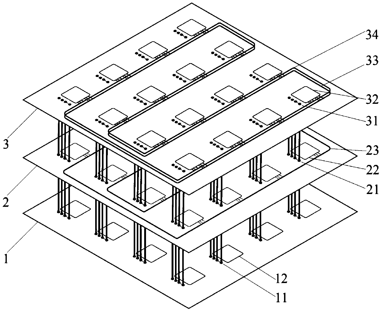
[0058] refer to figure 1 , a three-dimensional optical network on chip based on ring control optical network, including electrical layer 1, optical transmission network layer 2 and optical control network layer 3, the three layers 1, 2 and 3 form a stacked structure, and the relative positions of the three layers Not fixed, there can be the following six stacking methods from bottom to top: 1) Electrical layer 1-optical transmission network layer 2-optical control network layer 3, 2) electrical layer 1-optical control network layer 3-optical transmission network layer 2, 3) Optical transmission network layer 2-electrical layer 1-optical control network layer 3, 4) optical transmission network layer 2-optical control network layer 3-electrical layer 1, 5) optical control network layer 3-electrical layer 1- Optical transmission network...


PUM


Abstract

The invention provides a three-dimensional optical network-on-chip based on a ring control optical network and a communication method thereof for solving the technical problems of singleness of a wavelength using method and the like in the prior art. The three-dimensional optical network-on-chip comprises an electric layer, an optical transmission network layer and an optical control network layer, wherein the electric layer comprises N clusters, the optical transmission network layer comprises N transmitting / receiving units connected by a ring transmission optical waveguide, the optical control network layer comprises N control units connected with a ring notice optical waveguide and a ring arbitration optical waveguide respectively, the three layers form a stacked structure, and the three-dimensional optical network-on-chip is formed by connecting TSV (Through Silicon Vias) with a TSV pad; the three-dimensional optical network-on-chip dynamically adjusts the quantity of wavelengths used when data packets are transmitted according to the length of the data packets and the magnitude of a network load, and arbitrates wavelength resources used when data packets are transmitted in a manner of absorbing or releasing optical pulse signals, thereby realizing intra-cluster communication, inter-cluster communication and multicast / broadcast communication between IP cores.

Description

technical field [0001] The invention belongs to the technical field of communication, and relates to an optical on-chip network system and a communication method, in particular to a three-dimensional optical on-chip network based on a ring control optical network and a communication method thereof, which can be used for on-chip multi-core communication. Background technique [0002] Limited by physical limits, it is no longer feasible to improve the performance of single-core processors simply by reducing transistor size and increasing frequency. Adopting multi-core architecture design is an inevitable trend in the future development of System-on-Chip (SoC). The focus has shifted from multi-core system design to many-core or even thousand-core system design. With the increasing number of IP (Intellectual Property) cores integrated in SoCs, inter-core communication issues become the key to multi-core system design. Network-on-Chip (NoC) with good communication performance, g...

Claims


Application Information

Patent Timeline
Patent Type & Authority Patents(China)
IPC IPC(8): H04Q11/00G06F15/173G06F15/78
Inventor 顾华玺张博文王琨杨银堂朱樟明齐世雄谭伟
Owner XIDIAN UNIV
Why Eureka
Try Eureka