Pad area structure of liquid crystal panel

A liquid crystal panel, pad area technology, applied in nonlinear optics, instruments, optics, etc., can solve problems such as poor adhesion of conductive PAD, liquid crystal display not working properly, and FPC signals not being able to be effectively introduced into the panel.

Active Publication Date: 2017-01-18
WUHAN CHINA STAR OPTOELECTRONICS TECH CO LTD
View PDF6 Cites 9 Cited by
  • Summary
  • Abstract
  • Description
  • Claims
  • Application Information

AI Technical Summary

Problems solved by technology

[0007] In view of the above-mentioned problems in the prior art, this application proposes a pad area structure of a flexible circuit board of a liquid crystal display, which effectively solves the problem of

Method used


Image

  • Pad area structure of liquid crystal panel
  • Pad area structure of liquid crystal panel
  • Pad area structure of liquid crystal panel

Examples


Embodiment Construction

[0038] The present invention will be further described below in conjunction with accompanying drawing.

[0039] The implementation of the present invention will be described in detail below in conjunction with the accompanying drawings and examples, so as to fully understand and implement the process of how to apply technical means to solve technical problems and achieve technical effects in the present invention. It should be noted that, as long as there is no conflict, each embodiment and each feature in each embodiment of the present invention can be combined with each other, and the formed technical solutions are all within the protection scope of the present invention.

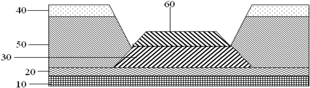
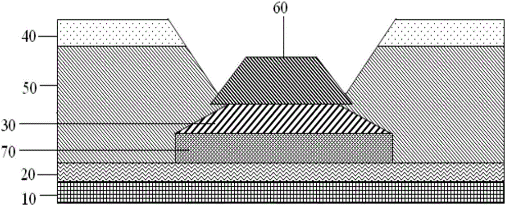
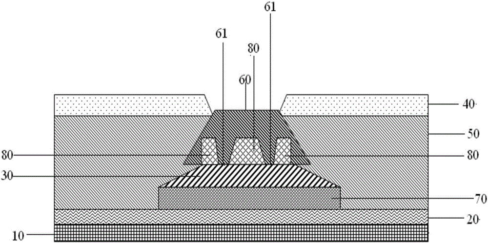
[0040] The present invention proposes a preferred embodiment, such as figure 2 As shown, specifically, it is a pad region structure of a liquid crystal panel, which is located in the concave portion formed by the flat layer 50 in the non-display area of ​​the liquid crystal panel, and the interlayer insu...


PUM


Abstract

The invention provides a pad area structure of a liquid crystal panel. The pad area structure is located in a concave part formed by a flat layer in a non-display area of the liquid crystal panel, and comprises an interlayer insulating layer, a second metal layer and an upper conductive layer, wherein the second metal layer is arranged on the interlayer insulating layer, and the upper conductive layer is arranged on the second metal layer; and the distance between the upper surface of the upper conductive layer and the upper surface of a first passivation protective layer is within a preset range. The pad area structure solves the problems that a conductive PAD of an LCD (Liquid Crystal Display) and a conductive PAD of an FPC (Flexible Printed Circuit) are not stuck well, signals of the FPC cannot be effectively guided into the panel, and the LCD cannot work normally. The interlayer insulating layer and the passivation protective layer are reserved in the sticking area of the conductive PAD of the LCD and the conductive PAD of the FPC to reduce the height difference between the sticking conductive layer and the circumference, so that the conductive PAD of the FPC and the conductive PAD of the LCD are well stuck, and signals of the FPC can be effectively guided into the panel of the LCD.

Description

technical field [0001] The invention relates to the field of display, in particular to a pad region structure of a low-temperature polysilicon liquid crystal display panel. Background technique [0002] Liquid crystal display is currently the most widely used flat-panel display, and has gradually become a display device with high-resolution color screens widely used in various electronic devices such as mobile phones, personal digital assistants (PDAs), digital cameras, computer screens or notebook computer screens. monitor. With the development and progress of liquid crystal display technology, people put forward higher requirements for the display quality, appearance design, human-machine interface, etc. of the liquid crystal display. [0003] At present, glass substrates used in liquid crystal display devices are generally amorphous silicon (a-Si) structures. However, with the advancement of technology, the technology of liquid crystal display panels with low temperature...

Claims


Application Information

Patent Timeline
IPC IPC(8): G02F1/1345
CPCG02F1/13458
Inventor 张启沛余赟
Owner WUHAN CHINA STAR OPTOELECTRONICS TECH CO LTD
Why Eureka
Try Eureka