Chuck working table and cleaning device

A technology of chuck workbench and cleaning device, which is applied in the manufacture of electrical components, circuits, semiconductors/solid-state devices, etc., and can solve problems such as deformation and damage

Active Publication Date: 2017-01-18
DISCO CORP
View PDF13 Cites 3 Cited by
  • Summary
  • Abstract
  • Description
  • Claims
  • Application Information

AI Technical Summary

Problems solved by technology

[0007] However, in the chuck table disclosed in Japanese Patent Application Laid-Open No. 2010-283286, since the suction holding part is not porous, but a plurality of grooves for suction are formed on the holding part to suction and hold the wafer, so in very In the case of a thin wafer, there is a fear that the wafer will be deformed and damaged just by suctioning the groove

Method used


Image

  • Chuck working table and cleaning device
  • Chuck working table and cleaning device
  • Chuck working table and cleaning device

Examples


Embodiment Construction

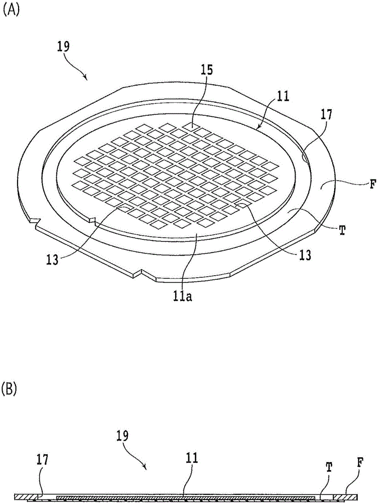
[0019] Hereinafter, embodiments of the present invention will be described in detail with reference to the drawings. when referring to figure 1 (A), a perspective view of the wafer unit 19 is shown. figure 1 (B) is a sectional view of the wafer unit 19 .

[0020] On the front surface of a semiconductor wafer (hereinafter simply referred to as a wafer) 11, a plurality of dividing lines (streets) 13 are formed in a grid pattern, and devices 15 such as ICs and LSIs are formed in each area divided by the dividing lines 13. .

[0021] The wafer unit 19 is configured such that the back surface of the wafer 11 is bonded to a dicing tape T serving as an adhesive tape, and the outer peripheral portion of the adhesive tape is bonded to the ring frame F so as to cover the opening 17 of the ring frame F. That is, in the wafer unit 19 , the wafer 15 is supported by the ring frame F via the dicing tape T. As shown in FIG.

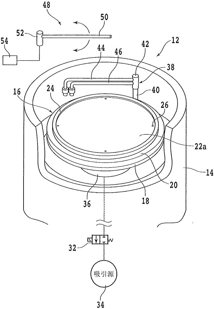
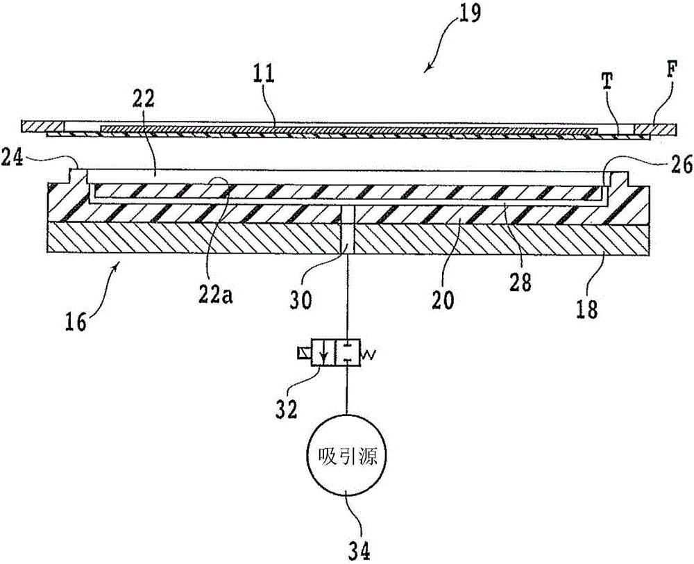
[0022] refer to figure 2 , shows a partially cutaway perspect...


PUM


Abstract

The invention provides a chuck working table and a cleaning device. When a wafer is very thin, the wafer can still be attracted and maintained on the premise that the wafer is not damaged. A wafer unit is maintained by the chuck working table; in the wafer unit, the wafer is supported by an adhesion belt; and the adhesion belt is adhered on an annular frame by covering an opening of the annular frame. The chuck working table comprises a sunk part, multiple attraction holes, and an attraction route, wherein the opening of the sunk part is smaller than the opening of the annular frame and larger than the diameter of the wafer, and the sunk part comprises a plat bottom face; the attraction holes are formed in the bottom face or an inner circumferential face of the sunk part of an area around the wafer which is maintained at a distance from the adhesion belt; the attraction route communicates the multiple attraction holes with an attraction source; when the wafer unit is to be maintained, a negative pressure is generated on the sunk part covered by the adhesion belt, and the wafer can be attracted and maintained on the bottom face at a distance from the adhesion belt.

Description

technical field [0001] The present invention relates to a chuck table and a cleaning device using the chuck table. Background technique [0002] With the miniaturization of electronic equipment, wafers such as semiconductor wafers are processed into thinner and smaller device chips. As a wafer, the back surface of the wafer is ground to a thickness of 100 μm or less in a grinding device, and is divided into individual device chips by a cutting device, a laser processing device, or the like. [0003] When cutting a thinned wafer, a wafer unit is formed in which the wafer is fixed to a ring frame with an adhesive tape, that is, a dicing tape, in order to improve workability. In addition, the wafer is held on the chuck table via the dicing tape of the wafer unit. Generally, a chuck table having a holding surface made of a porous ceramic material is used, and the suction force acts uniformly and in balance to hold the wafer. . [0004] However, with the chuck table whose hold...

Claims


Application Information

Patent Timeline
Patent Type & Authority Applications(China)
IPC IPC(8): H01L21/683H01L21/67
CPCH01L21/67023H01L21/6836H01L21/6838H01L21/6833H01L21/02052H01L21/6704H01L21/6831
Inventor 新田秀次瓜田直功八木原惇江角和也
Owner DISCO CORP
Why Eureka
Try Eureka