

Planar Single-Chip Inertial Measurement Combination
An inertial measurement and single-chip technology, applied in the field of micro-inertial devices, can solve the problems of large processing errors and high processing technology requirements, and achieve the effects of reducing plate-making costs, avoiding lag effects, and reducing difficulty
Inactive Publication Date: 2012-07-18
NORTHWESTERN POLYTECHNICAL UNIV
View PDF1 Cites 0 Cited by
- Summary
- Abstract
- Description
- Claims
- Application Information
AI Technical Summary
Problems solved by technology
The purpose of the present invention is to provide a planar single-chip inertial measurement combination that can effectively avoid the lag effect, thereby overcoming the problems that the existing planar single-chip inertial measurement combination has high requirements for processing technology and large processing errors
Method used
View moreImage
Smart ImageViewing Examples

Examples
Embodiment 1
Embodiment 2
Login to View More PUM
 Abstract
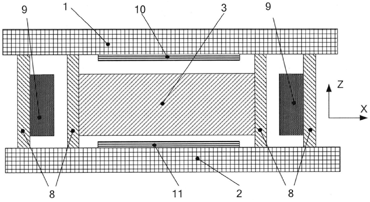
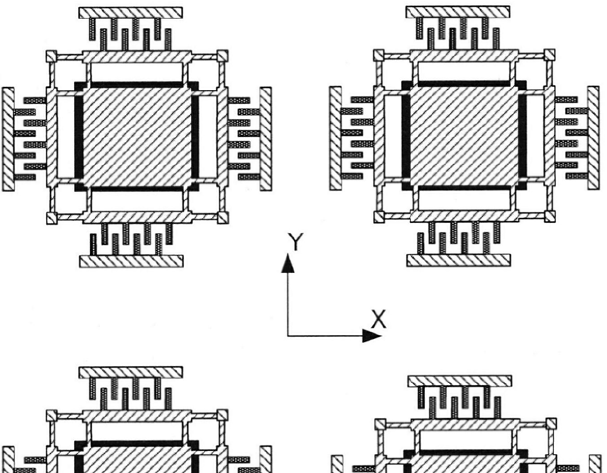
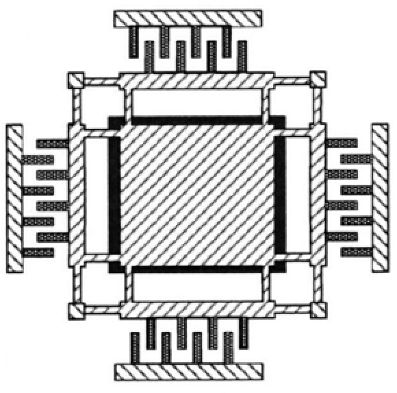
The invention discloses a planar single-chip inertial measurement combination, which belongs to the technical field of micro-inertial devices. The planar single-chip inertial measurement combination contains at least two planar inertial sensors with the same structure; each planar inertial sensor includes an upper base, a structural layer and a lower base parallel to each other. The structure layer is connected with the upper base and the lower base through the bonding block and forms a suspended structure. An upper electrode and a lower electrode are respectively arranged on the upper base and the corresponding position of the upper base and the inertial mass block; the upper electrode, the inertial mass block and the lower electrode form a differential capacitor. The inertial measurement combination of the present invention is composed of the same device, which reduces the difficulty of process design of multiple heterogeneous devices and avoids the lag effect as much as possible. In addition, in the manufacturing process, a single device can be used for mask manufacturing, and various devices can be combined by dicing, which reduces the cost of plate making.
Description
Planar Single-Chip Inertial Measurement Combination technical field The invention provides a planar single-chip inertial measurement combination, which belongs to the technical field of micro-inertial devices. Background technique The U.S. Milli Sensor Systems & Actuators company announced a planar single-chip inertial measurement combination in the U.S. patent No. 6859751, and each planar inertial sensor that constitutes the planar single-chip inertial measurement combination, that is, the working principle of the gyroscope and the accelerometer is the same , with a similar structure. The planar-type single-chip inertial measurement combination includes multiple planar inertial sensors processed at one time by the same micro-processing technology to form a single-chip micro-inertial measurement combination, which has the characteristics of high alignment and low cost. Although the various planar inertial sensors included in the planar single-chip inertial measurement co...
Claims
Login to View More Application Information
Patent Timeline
 Patent Type & AuthorityPatents(China)
IPC IPC(8): G01P15/125G01P3/44
Inventor苑伟政蒋庆华吕湘连常洪龙
OwnerNORTHWESTERN POLYTECHNICAL UNIV