On-line diagnosis method for defects in laser material increasing manufacturing process on basis of spectrum diagnosis
A laser additive, manufacturing process technology, used in materials excitation analysis and other directions
- Summary
- Abstract
- Description
- Claims
- Application Information
AI Technical Summary
Problems solved by technology
Method used
Image
Examples
Embodiment 1
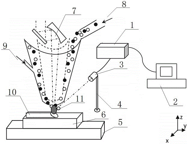
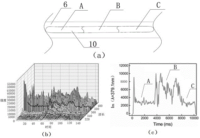
[0043] In this example, the schematic diagram of the additive molding object formed by laser additive manufacturing is as follows: image 3 As shown in (a), the molding layer 10 is divided into a first area A, a second area B, and a third area C, and the molding layer 10 in the first area A and the third area C is protected by Ar during the manufacturing process. Ar shielding gas 9 is used for protection, while the molding layer 10 of the second region B is not protected by Ar shielding gas 9 during the manufacturing process. This situation is to simulate the situation when the shielding gas changes greatly during the production process.
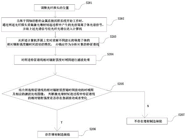
[0044] During the manufacturing process of laser additive materials, the optical fiber probe 3 is used to collect the photoplasma spectral information in the wavelength range of 200~1100nm in the laser additive manufacturing process, and the above spectral information is sent to the computer 2 through the optical fiber spectrometer 1 , Throu...
Embodiment 2
[0048] In this embodiment, the schematic diagram of the additive molding object formed by laser additive manufacturing is as follows Image 6 As shown in (a), the molding layer 10 is divided into a fourth area D, a fifth area E, a sixth area F and a seventh area G, and the molding layer 10 in the fourth area D and the sixth area F is manufactured The output power of the laser in the process is 1200W, and the output power of the laser in the manufacturing process of the forming layer 10 of the fifth region E and the seventh region G is 700W. This situation is to simulate the output power of the laser in the production process. case of large changes.
[0049] Based on the relative radiation intensity of the characteristic spectral line FeI384.0nm, a time-domain diagram corresponding to the additive manufacturing process is established, such as Image 6 As shown in (b), it can be seen from the figure that when the state of the graph fluctuates or changes sharply from the relativ...
Embodiment 3
[0051] In this embodiment, the schematic diagram of the additive molding object formed by laser additive manufacturing is as follows Figure 7 As shown in (a), the molding layer 10 is divided into the eighth area H, the ninth area I and the tenth area J, and the scanning speed of the molding layer 10 in the eighth area H and the tenth area J during the manufacturing process is is 5 mm / s, while the scanning speed of the molding layer 10 in the ninth region I is lower than 5 mm / s during the manufacturing process, this situation is the case of simulating a large change in the scanning speed during the production process.
[0052] Based on the relative radiation intensity of the characteristic spectral line FeI384.0nm, a time-domain diagram corresponding to the additive manufacturing process is established, such as Figure 7 As shown in (b), it can be seen from the figure that when the state of the graph fluctuates or changes sharply from the relatively stable state of the eighth ...
PUM
 Abstract
Description
Claims
Application Information


