
Open structure, manufacturing method thereof and interconnect structure

A technology with an opening structure and a manufacturing method, which is applied in the manufacturing of semiconductor/solid-state devices, electrical components, and electrical solid-state devices, etc., can solve the problems of reduced process margin, ineffective connection between contact windows and pads, etc., to improve the process margin. degree of effect

Active Publication Date: 2017-01-25
MACRONIX INT CO LTD
View PDF3 Cites 4 Cited by
  • Summary
  • Abstract
  • Description
  • Claims
  • Application Information

AI Technical Summary

Problems solved by technology

[0005] In this way, since the thickness of the etch stop layer is greatly increased, the space of the contact window will be compressed and the process window will be reduced, so that the contact window and the pad cannot be effectively connected.

Method used


Image

  • Open structure, manufacturing method thereof and interconnect structure
  • Open structure, manufacturing method thereof and interconnect structure
  • Open structure, manufacturing method thereof and interconnect structure

Examples


Embodiment Construction

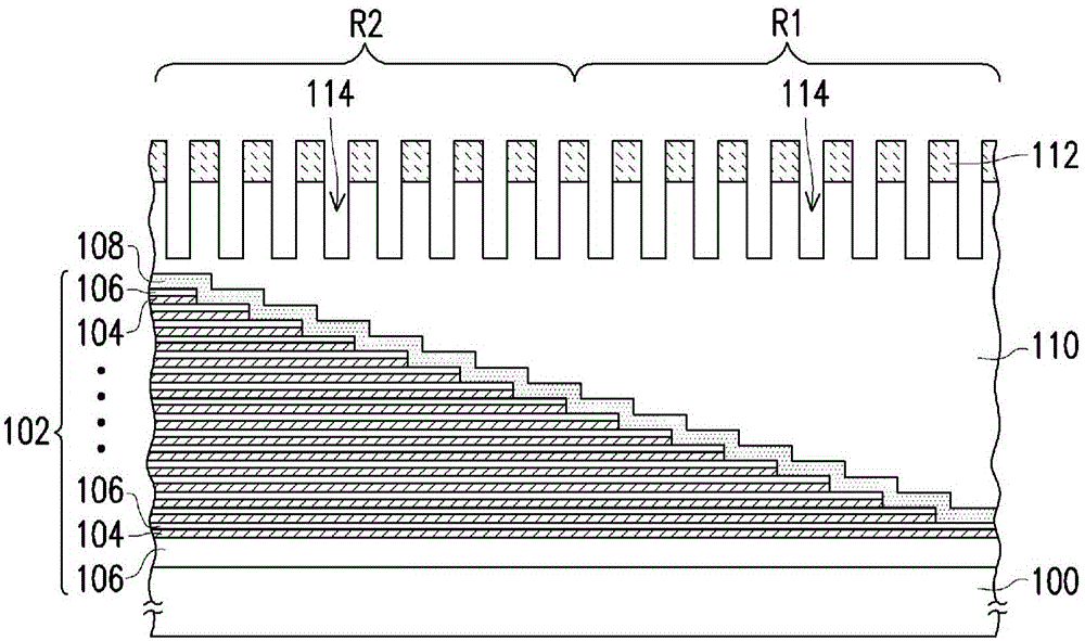
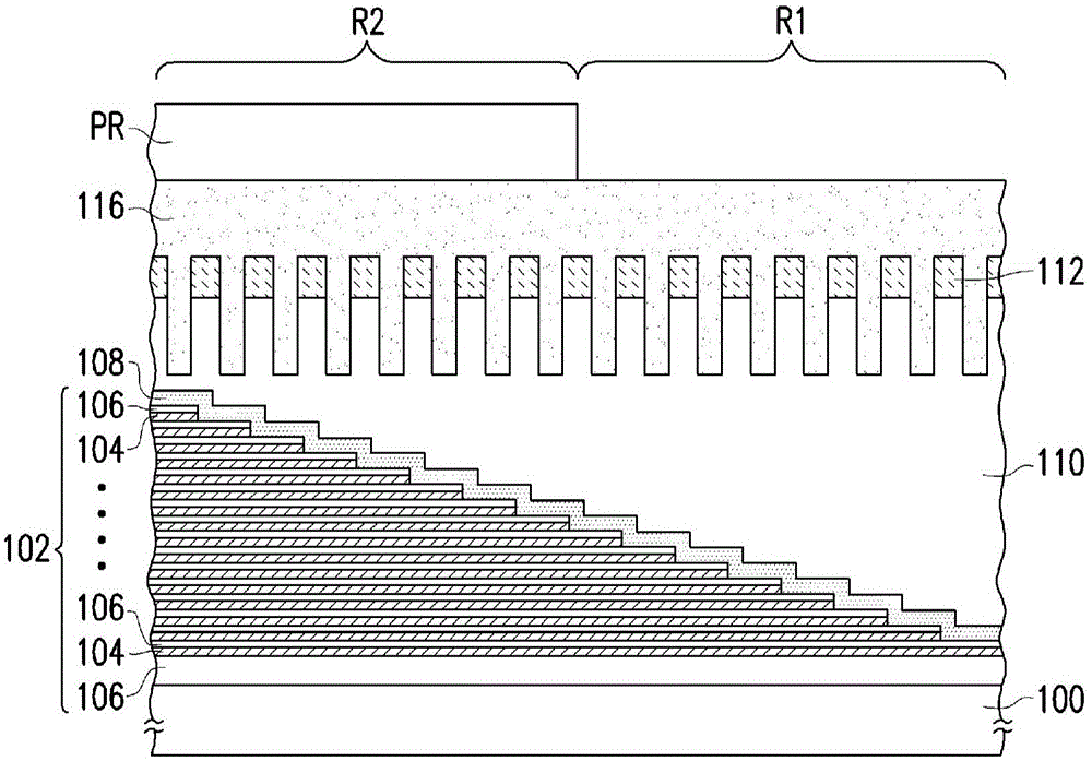
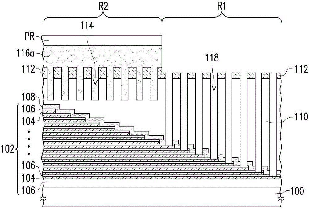
[0048] Figure 1A to Figure 1H It is a cross-sectional view of the manufacturing process of the interconnection structure according to an embodiment of the present invention.

[0049] First, please refer to Figure 1A , forming a multilayer structure 102 on the substrate 100 . The multi-layer structure 102 includes multiple layers of conductive layers 104 and multiple layers of dielectric layers 106 stacked alternately. The height of the conductor layer 104 located in the first region R1 is lower than that of the conductor layer 104 located in the second region R2. In this embodiment, the multilayer structure 102 is described by taking a ladder structure as an example, but the present invention is not limited thereto, as long as the multilayer structure 102 can be partitioned according to the height of the conductor layer 104, it belongs to the scope of the present invention. scope of protection. In addition, although this embodiment is described by taking a first region R1...


PUM


Abstract

The invention provides a manufacturing method of an open structure. The manufacturing method includes the steps of forming a multi-layer structure on a substrate, wherein the multi-layer structure comprises conductor layers and first dielectric layers which are stacked alternately, and the conductor layers in a first region are lower than the conductor layers in a second region; forming second dielectric layers covering the multi-layer structure; forming patterned mask layers on the second dielectric layers; forming first fill-in layers in the second region, wherein the first fill-in layers cover the second dielectric layers exposed over the patterned mask layers; taking the first fill-in layers and the patterned mask layers as masks to form a plurality of first openings of the conductor layers exposed over the first region; removing the first fill-in layers; forming second fill-in layers for filling the first openings; taking the second fill-in layers and the patterned mask layers as masks to form a plurality of second openings of the conductor layers exposed over the second region. The invention further provides the opening structure and an interconnect structure.

Description

technical field [0001] The present invention relates to an opening structure, a manufacturing method thereof, and an interconnection structure, and in particular to an opening structure applicable to a three-dimensional semiconductor element, a manufacturing method thereof, and an interconnection structure. Background technique [0002] With the integration of semiconductor components, in order to achieve the goal of high density and high performance, it has become a trend to develop into three-dimensional space within a limited unit area. Common three-dimensional semiconductor elements such as three-dimensional NAND flash memory (3D-NAND flash memory) in non-volatile memory. [0003] Taking the multi-layer device of the three-dimensional NAND flash memory as an example, the stepped multi-layer pad structure enables the contact windows to be respectively connected to different film layers in the multi-layer device. Since the aspect ratios of the shallowest and deepest conta...

Claims


Application Information

Patent Timeline
Patent Type & Authority Applications(China)
IPC IPC(8): H01L21/60H01L23/485
CPCH01L23/485H01L24/83
Inventor 龙成一
Owner MACRONIX INT CO LTD
Learn More