Semiconductor wafer notch groove crystal orientation measuring device and use method
A technology for measuring devices and semiconductors, which is applied in the fields of measuring devices, material analysis using radiation diffraction, and material analysis using wave/particle radiation, etc. Accurate, efficient and easy to operate
- Summary
- Abstract
- Description
- Claims
- Application Information
AI Technical Summary
Problems solved by technology
Method used
Image

Examples
Embodiment Construction
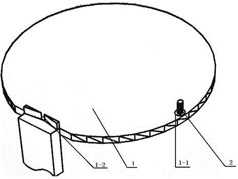
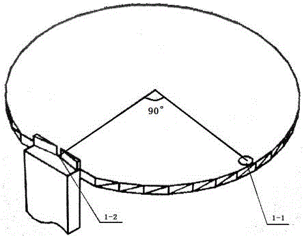
[0009] Further explanation will be given below in conjunction with the accompanying drawings and taking a 6-inch semiconductor wafer with a crystal orientation, a diameter of 151mm, and positions 1-10 of the main reference as examples.
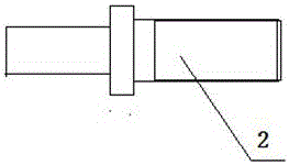
[0010] Such as figure 1 , 2 , 3, the positioning column hole 1-1 on the circular worktable of the YX-2D6 model X-ray orientation instrument 1 is a threaded hole with a groove, and the center of the circle is at the X-ray measurement point on the circular worktable ( 1-2) Take the line connecting the center of the measuring platform as the reference line, rotate the outer circle 90° counterclockwise, and take D–r as the radius. The positioning post hole 1-1 is an M3 threaded hole with a diameter of 3mm and a height of The notch groove positioning column 2 is a cylinder composed of a M3 threaded body with a length of 6mmd, a cylinder with a diameter of 3mm and a height of 1mm, and a smooth cylinder with a diameter of 2.2mm and a height of 11mm...
PUM
 Abstract
Description
Claims
Application Information
 - R&D
- Intellectual Property
- Life Sciences
- Materials
- Tech Scout
- Unparalleled Data Quality
- Higher Quality Content
- 60% Fewer Hallucinations
Browse by: Latest US Patents, China's latest patents, Technical Efficacy Thesaurus, Application Domain, Technology Topic, Popular Technical Reports.
© 2025 PatSnap. All rights reserved.Legal|Privacy policy|Modern Slavery Act Transparency Statement|Sitemap|About US| Contact US: help@patsnap.com