Infrared camouflage material
A stealth material, infrared technology, applied in the field of infrared stealth
- Summary
- Abstract
- Description
- Claims
- Application Information
AI Technical Summary
Problems solved by technology
Method used
Image
Examples
Embodiment 1
[0030] Fabrication of Alternately Arranged YbF on Substrate by Ion Beam Sputtering 3 film and ZnSe film, the bottom and top layers are both YbF 3 The number of layers of the multilayer film is 33, and the thickness of the film from the bottom layer is 0.97453 μm, 0.64834 μm, 0.39490 μm, 0.44593 μm, 0.43009 μm, 0.54081 μm, 1.10301 μm, 0.12082 μm, 0.66528 μm, 0.61058 μm ,0.90684μm,0.10666μm,0.83247μm,0.57832μm,0.7648μm,0.17861μm,0.81283μm,0.44699μm,1.91144μm,1.02709μm,0.68401μm,0.26756μm,0.50729μm,0.40487μm,1.026μm,0.05128μm,0.56253 μm, 1.24633μm, 0.48934μm, 0.44942μm, 0.39864μm, 0.29366μm, 1.63612μm.
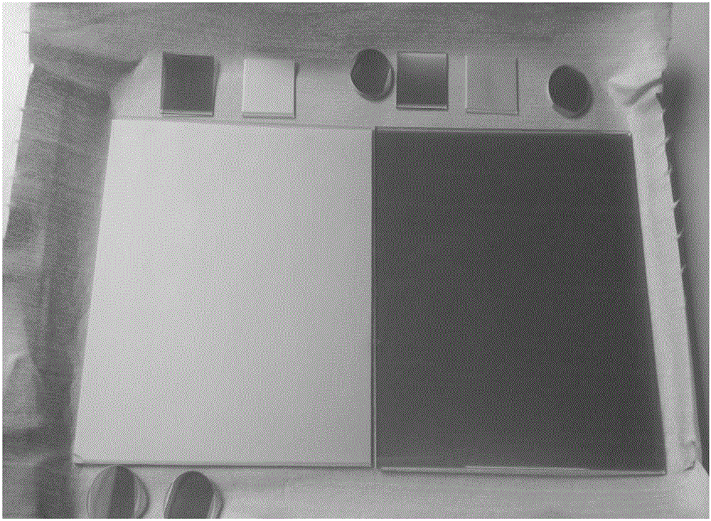
[0031] The prepared infrared stealth material flat sample such as figure 1 shown.
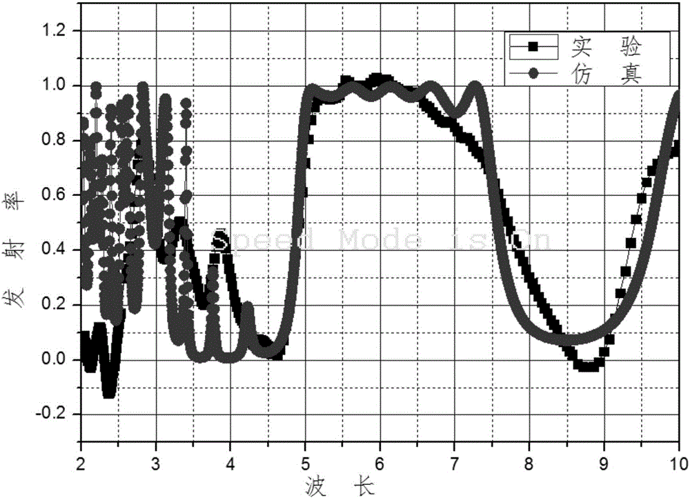
[0032] The infrared stealth performance of the infrared stealth material was tested and verified by Fourier transform infrared spectrometer, and the comparison chart of the emissivity simulation and test curve in the infrared band was obtained, as shown in figure 2 shown. from figure 2It c...
PUM
 Abstract
Description
Claims
Application Information
 - R&D
- Intellectual Property
- Life Sciences
- Materials
- Tech Scout
- Unparalleled Data Quality
- Higher Quality Content
- 60% Fewer Hallucinations
Browse by: Latest US Patents, China's latest patents, Technical Efficacy Thesaurus, Application Domain, Technology Topic, Popular Technical Reports.
© 2025 PatSnap. All rights reserved.Legal|Privacy policy|Modern Slavery Act Transparency Statement|Sitemap|About US| Contact US: help@patsnap.com


