
Laser etching circuit structure of touch panel

A circuit structure, touch panel technology, applied in the direction of instrument, electrical digital data processing, data processing input/output process, etc., can solve problems such as disconnection, inconsistent line width of trace 33, deviation of laser moving path 32, etc.

Active Publication Date: 2017-02-08
INTERFACE TECH CHENGDU CO LTD +2
View PDF2 Cites 1 Cited by
  • Summary
  • Abstract
  • Description
  • Claims
  • Application Information

AI Technical Summary

Problems solved by technology

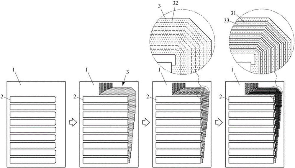
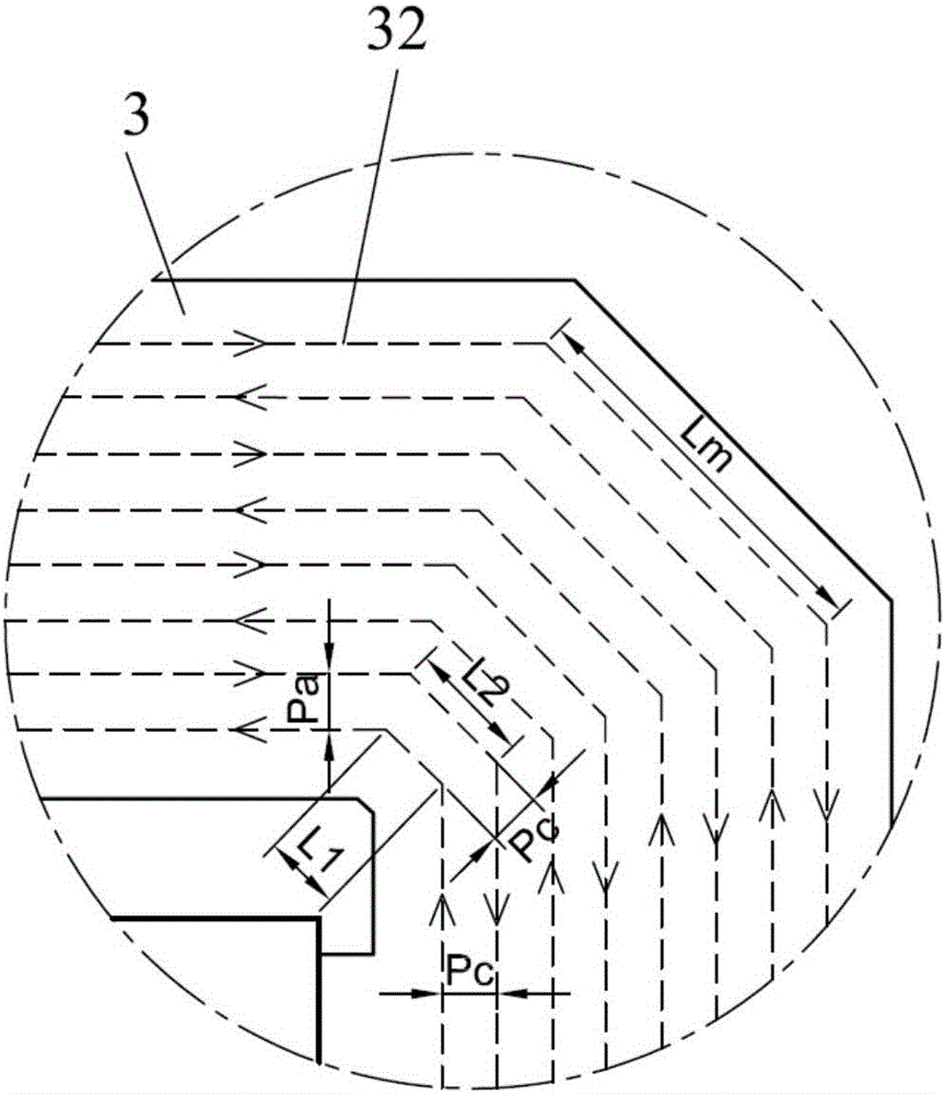
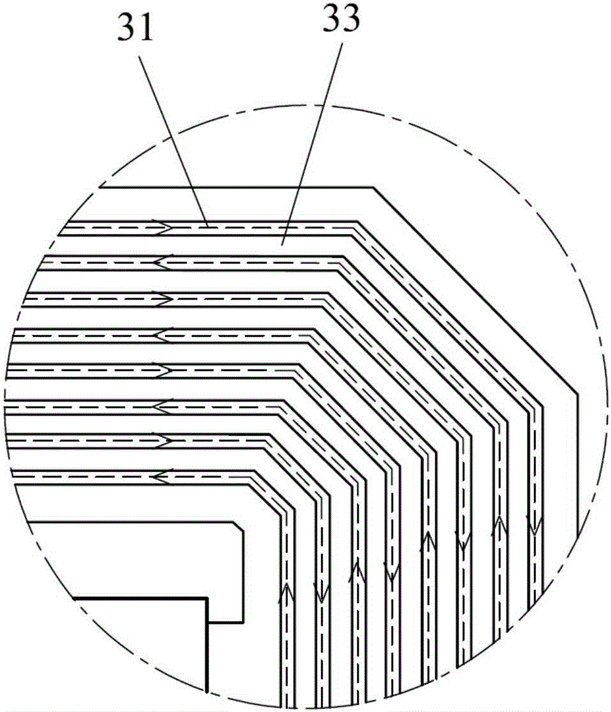
However, when the laser etching line 31 has a very small line spacing (less than 80 microns) and the laser scanning speed is fast, the two vibrating mirrors move at the same time at the corner, and the laser moving path 32 is prone to deviate at this time, causing the line spacing (Pa, Pb, Pc) are not equal, such as Figure 4 As shown, the line width of the line 33 will be inconsistent, resulting in the problem that the line 33 is too thin or broken. At this time, the scanning speed must be reduced to reduce the production capacity, so there is still room for improvement.

Method used


Image

  • Laser etching circuit structure of touch panel
  • Laser etching circuit structure of touch panel
  • Laser etching circuit structure of touch panel

Examples


Embodiment Construction

[0015] In order to achieve the above-mentioned purpose and effect, the technical means and structure adopted in this creation are hereby drawn to illustrate in detail the characteristics and functions of the preferred embodiment of this creation as follows, so that Li can fully understand it, but it should be noted that these contents are not constituting the limitations of the invention.

[0016] Please also see Figure 5 , Image 6 and Figure 7 As shown, it is a structural schematic diagram, a partial circuit schematic diagram, and a partial circuit enlarged schematic diagram of a preferred embodiment of the laser-etched circuit structure of the touch panel of the invention. The invention provides a laser etching circuit structure of a touch panel, which is located on a touch substrate 1 and is connected to a plurality of transparent electrodes 2 in telecommunications. The laser etching circuit structure of the touch panel includes a main circuit area 5 and a plurality of...


PUM


Abstract

The invention discloses a laser etching circuit structure of a touch panel. The laser etching circuit structure of the touch panel comprises a plurality of laser etching line bodies and a plurality of screen-printed silver paste lines. The laser etching line bodies include first line bodies, second line bodies and third line bodies. The central paths of the two first line bodies are spaced by a first width; the central paths of the two second line bodies are spaced by a second width; the third line bodies are connected with one ends of the first line bodies and one ends of the second line bodies; the central paths of the two third line bodies are spaced by a third width; and each screen-printed silver paste line is located between the two laser etching line bodies. The third line bodies are same in length dimension, the first width and the second width are same in length dimension, and the length dimension of the third width is greater than that of the first width. Through the structure, the shortcoming of excessively small thickness or line breakage of the screen-printed silver paste lines (routing lines) caused by inconsistent line widths of the routing lines due to excessively small line spacing of the routing lines or relatively quick laser etching in a fabrication process can be improved.

Description

technical field [0001] The present invention relates to a laser etching circuit structure of a touch panel, in particular to a method of enlarging the line spacing of the hypotenuse in the limited space at the corner of the laser screen printing silver paste line, and improving the line spacing caused by the conventional process. The laser etched circuit structure of the touch panel with inconsistent line width caused by too small spacing. Background technique [0002] At present, various mobile phones, media players, navigation systems, digital cameras and other electronic products on the market are beginning to be equipped with various types of touch screens. According to their principles, they can be divided into resistive, capacitive, infrared and surface acoustic wave. Capacitive touch screens (hereinafter referred to as capacitive screens) are the most common. The functional layer of the capacitive screen is mainly composed of transparent conductive electrodes located...

Claims


Application Information

Patent Timeline
IPC IPC(8): G06F3/044
CPCG06F3/044
Inventor 张轩满
Owner INTERFACE TECH CHENGDU CO LTD
Learn More