Stripping method and stripping device

A stripping device and stripping starting point technology, which is applied to semiconductor devices, electrical components, circuits, etc., can solve the problems of protective tape blockage, high operating cost of stripping tape, and complicated structure, and achieve the effect of suppressing operating costs

Active Publication Date: 2021-10-29
DISCO CORP
View PDF10 Cites 0 Cited by
  • Summary
  • Abstract
  • Description
  • Claims
  • Application Information

AI Technical Summary

Problems solved by technology

[0007] In the peeling device of the protective tape based on the above-mentioned prior art, there is the following problem: since the protective tape is stuck on the front surface of the semiconductor wafer due to the pressing force generated during the grinding process, it becomes difficult to peel the protective tape from the front surface of the semiconductor wafer. In the case of a protective tape, a peeling tape exhibiting a strong adhesive force is attached to the protective tape, and the peeling tape is pulled to peel off the protective tape. In order to realize this structure, at least a conveying mechanism for the peeling tape, The structure of the cutting mechanism of the peeling tape and the crimping mechanism of the peeling tape becomes complicated
Furthermore, the following problems have also arisen: as described above, a strong adhesive force is required for the peeling tape, and it is required to withstand the strength of the peeling process of the firmly attached protective tape. The operating cost of the peeling tape of the peeling device becomes high
[0008] In addition, in the above-mentioned conventional technology, there is a problem in that after the peeling tape is bonded to the end of the protective tape by pressure and peeled, the peeled protective tape is discarded in the waste container of the peeling device. , the adhesive surface of the peeling tape will adhere to the side wall of the waste container, regardless of whether there is any remaining capacity in the waste container, the peeled protective tape will block the opening of the waste container, and the capacity of the waste container cannot be fully utilized.

Method used


Image

  • Stripping method and stripping device
  • Stripping method and stripping device
  • Stripping method and stripping device

Examples


Embodiment Construction

[0036] Hereinafter, preferred embodiments of a peeling method according to the present invention and a peeling device for performing the peeling method will be described in detail with reference to the drawings.

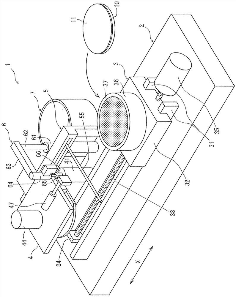
[0037] exist figure 1 A perspective view of an embodiment of a peeling device 1 constructed according to the present invention is shown in . The peeling device 1 in the illustrated embodiment includes a stationary base 2 , a holding table mechanism 3 , a sheet holding unit 4 , a bending roller moving unit 5 , a peeling starting point generating unit 6 , and a waste container 7 .

[0038] As shown in the figure, the holding table mechanism 3 includes: two guide rails 31, 31, which are arranged on the stationary base 2 along the feeding direction (peeling direction) of the peeling process shown by arrow X; 32, which is slidably arranged on the two guide rails 31, 31; the ball screw shaft 33, which is engaged with the nut portion on the lower surface of the mobile base...


PUM


Abstract

Provided are a peeling method and a peeling device capable of peeling a protective tape (sheet) affixed to a semiconductor wafer (plate member) without using a peeling tape with a complicated structure and a large burden on running costs. According to the present application, a peeling method and a peeling device capable of performing the peeling method are provided. The peeling method includes at least: a first peeling step of making the front end of the front needle-shaped member abut against the sheet of the plate-shaped member held by the holding table. At least a part of the outer periphery, so that this part is peeled from the plate-shaped member; the peeling starting point generation process blows air between the part of the peeled sheet and the plate-shaped member, and generates a part that includes the part. a peeling starting point formed by the enlarged peeling region; and a final peeling step of separating and peeling the unpeeled remaining portion of the sheet from the plate-shaped member starting from the peeling starting point.

Description

technical field [0001] The present invention relates to a peeling method and a peeling device for peeling a sheet adhered to a plate-like member such as a semiconductor wafer. Background technique [0002] In the manufacturing process of semiconductor devices, a plurality of regions are divided by dividing lines arranged in a grid pattern on the front surface of a substantially disk-shaped semiconductor wafer, and devices such as ICs and LSIs are formed in the divided regions. And, after the back surface of the semiconductor wafer is ground to a predetermined thickness by a grinding device, the semiconductor wafer is cut along a planned dividing line by a dicing device, a laser processing device, etc. Individual semiconductor devices are manufactured by dividing. [0003] In order to miniaturize semiconductor chips such as ICs and LSIs, it is preferable to make the back surface of the semiconductor wafer (plate-shaped member) as thin as possible in the above-mentioned grind...

Claims


Application Information

Patent Timeline
Patent Type & Authority Patents(China)
IPC IPC(8): H01L21/683
CPCH01L21/6836H01L2221/68318H01L21/7806H01L21/76H01L2924/35121
Inventor 高泽徹
Owner DISCO CORP
Why Eureka
Try Eureka