NAND memory structure, NAND memory structure formation method and three dimensional memory array

A memory and multi-layer storage technology, which is applied in the field of information storage, can solve the problems of high process complexity and achieve the effects of low process complexity, reduction of channel aperture, and increase of integration density

Active Publication Date: 2017-02-15
TSINGHUA UNIV
View PDF11 Cites 32 Cited by
  • Summary
  • Abstract
  • Description
  • Claims
  • Application Information

AI Technical Summary

Problems solved by technology

The "gate replacement" process adds multiple dielectric deposition and etching process steps, and the process complexity is very high

Method used


Image

  • NAND memory structure, NAND memory structure formation method and three dimensional memory array
  • NAND memory structure, NAND memory structure formation method and three dimensional memory array
  • NAND memory structure, NAND memory structure formation method and three dimensional memory array

Examples


Embodiment Construction

[0053] Embodiments of the present invention are described in detail below, examples of which are shown in the drawings, wherein the same or similar reference numerals designate the same or similar elements or elements having the same or similar functions throughout. The embodiments described below by referring to the figures are exemplary and are intended to explain the present invention and should not be construed as limiting the present invention.

[0054] A method for forming a NAND memory, a structure of a NAND memory and a method for forming the structure according to an embodiment of the present invention will be described below with reference to the accompanying drawings.

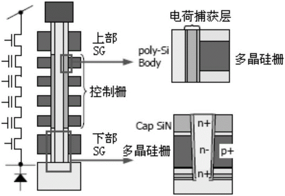
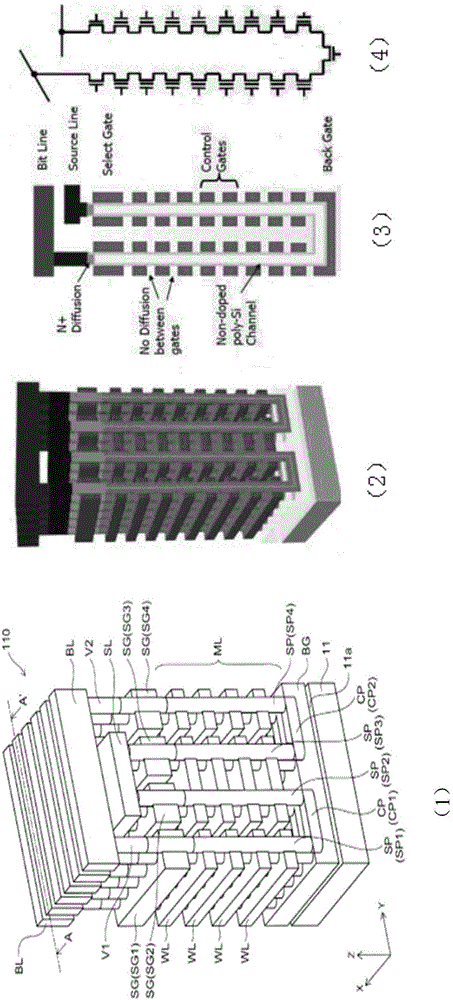
[0055] Figure 6 is a schematic diagram of the NAND memory structure according to an embodiment of the present invention, such as Figure 6 As shown, the NAND memory structure 100 includes a vertically stacked memory cell, a source select transistor and a bit line layer 400 (BL).

[0056] Among the...


PUM


Abstract

The invention discloses an NAND memory structure formation method. The formation method comprises the following steps of providing a semiconductor substrate, and forming multiple groups of source electrode selection transistors in the substrate; forming a storage unit of a vertical laminated structure on the source electrode selection transistors, wherein the storage unit of the vertical laminated structure comprises a vertical channel, a multi-layer storage gate medium, and a bit line selection tube grid and a laminated word line formed outside the vertical channel, and drain electrodes of the source electrode selection transistors are contacted with the multi-layer storage gate medium on the bottom of the vertical channel; and forming a bit line on the storage unit of the vertical laminated structure; and applying breakdown voltage to the multi-layer storage gate medium between the drain electrodes of the source electrode selection transistors and the vertical channel through the bit line and the laminated word line. The NAND memory structure formation method can reduce the process difficulty and the cost and improve the integration density. The invention also discloses an NAND memory structure and a formation method thereof and a three dimensional memory array.

Description

technical field [0001] The invention belongs to the technical field of information storage, and in particular relates to a method for forming a NAND memory, a structure of the NAND memory and a method for forming the same, and a three-dimensional NAND memory array. Background technique [0002] NAND memory technology continues to develop, its storage performance continues to improve, and many related technologies continue to propose new structural solutions. [0003] Among them, BiCS (Bit Cost Scalable) technology is "planar gate vertical channel" and "gate first, then channel" technology, refer to relevant literature, for example, [1], H.Tanaka et al., Bit Cost Scalable Technology with Punch and Plug Process for Ultra High Density Flash Memory, 2007Symposium on VLSI Technology Digest of Technical Papers, pp.14-15. [2], US7,852,675: Threedimensional stacked nonvolatile semiconductor memory, this patent describes the structural method of BICS vertical arrangement. Specifical...

Claims


Application Information

Patent Timeline
Patent Type & Authority Applications(China)
IPC IPC(8): H01L21/8247H01L27/115
CPCH10B43/35H10B43/20H01L28/00H10B69/00
Inventor 潘立阳
Owner TSINGHUA UNIV
Why Eureka
Try Eureka