Tapered super-surface structure based photovoltaic photoelectric detector and preparation method thereof

A photodetector and metasurface technology, applied in the field of photodetectors, can solve problems such as complex preparation process and angle sensitivity, and achieve the effect of high-efficiency photodetection and wide-angle photodetection

Active Publication Date: 2017-02-15
SOUTHEAST UNIV
View PDF2 Cites 24 Cited by
  • Summary
  • Abstract
  • Description
  • Claims
  • Application Information

AI Technical Summary

Problems solved by technology

[0005] Purpose of the invention: Aiming at the shortcomings of narrow band, angle sensitivity and complex preparation process of the existing photodetector based on thermionic principle, the present invention proposes a conical metasurface structure prepared by simple, mature and low cost, and designs a wide spectrum Wide Angle Photovoltaic Photodetector

Method used


Image

  • Tapered super-surface structure based photovoltaic photoelectric detector and preparation method thereof
  • Tapered super-surface structure based photovoltaic photoelectric detector and preparation method thereof
  • Tapered super-surface structure based photovoltaic photoelectric detector and preparation method thereof

Examples


Embodiment 1

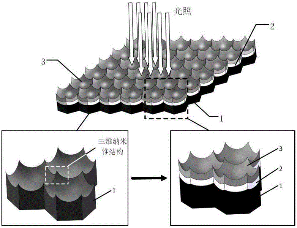
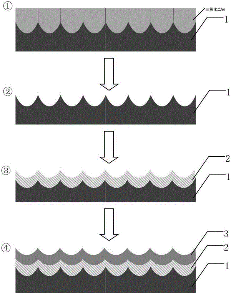
[0039] In order to realize a photodetector suitable for a wide spectrum and wide angle in the visible light region, the photodetector based on the tapered metasurface structure in this embodiment includes an aluminum substrate with a three-dimensional nanocone array structure on the surface, a titanium dioxide semiconductor layer, and a gold film layer . Wherein the gold thin film layer has a thickness of 20nm, and the titanium dioxide semiconductor layer has a thickness of 40nm. The nano cone array is a non-periodic array, the height of the nano cones is between 100-500nm, and the distance between the nano cones is kept between 100-500nm.

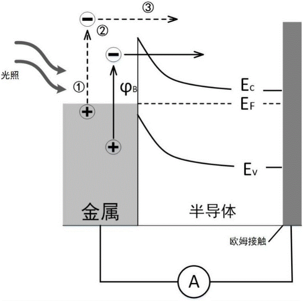
[0040] When the full band of visible light is incident on the cone-shaped upper surface of the detector, the conical metasurface structure is different from the common use of plasmon resonance modes or resonant cavities that can only achieve superabsorption at a single wavelength or a single incident angle. The metasurface structure, the wi...

Embodiment 2

[0048] In order to realize a photodetector suitable for a wide spectrum and wide angle in the near-infrared region, different from Embodiment 1, the semiconductor thin film layer of this embodiment is a silicon thin film, and the specific structural parameters are that the thickness of the gold thin film layer is 15nm, and the thickness of the silicon thin film is 15nm. The thickness of the layer is 50 nm. The nanocone array is a non-periodic array, the height of the nanocones is between 500-1000nm, and the distance between the nanocones is kept between 1000-2000nm. When the surface of the incident photodetector in the infrared region, because the conical metasurface structure is different from the metasurface structure that uses ordinary plasmon resonance modes or resonant cavities can only achieve superabsorption at a single wavelength or a single incident angle, this The wide-band and wide-angle superabsorption that can be realized by this kind of tapered structure.

[004...


PUM


Abstract

The invention discloses a tapered super-surface structure based photovoltaic photoelectric detector and a preparation method thereof. The photoelectric detector comprises a metal substrate whose surface includes a 3D nanometer cone array structure, a semiconductor file layer whose forbidden band width is greater than incident photon energy, and a metal film layer; and the metal substrate, the semiconductor film layer and the metal film layer are arranged successively from bottom to top. The preparation method comprises that a porous anodised aluminum film is prepared on the aluminum substrate, the anodised aluminum film in the surface of the aluminum substrate is removed, and the semiconductor film layer and the metal film layer are prepared then. The metal substrate, the semiconductor film layer and the metal film layer for the super-surface structure, the thickness of the metal film layer, the material thickness of the semiconductor layer or a structural parameter of a nanometer cone is controlled to regulate and control the frequency range of super-absorption. The photoelectric detector is simple in preparation technology, convenience is provided for large-area preparation, complex micro nano processing is not needed, and high-effeminacy broadband wide-angle photoelectric detection can be realized.

Description

technical field [0001] The invention belongs to the technical field of photodetectors, in particular to a photovoltaic photodetector based on a tapered metasurface structure and a preparation method thereof. Background technique [0002] The hot electrons generated by the plasmon resonance decay of the metal nanostructure are injected into the adjacent semiconductor to generate a photocurrent to realize a solid-state photodetector device, which was first confirmed by the Halas research group ("Science" volume 332, page 702), using this Based on this principle of photodetection, its detection band is not limited by the forbidden band width of the semiconductor, but is determined by the Schottky barrier formed between the metal and semiconductor, and its response spectrum can be adjusted by changing the metal nanostructure or material. Although there are many advantages based on this principle, the photoelectric conversion efficiency of photodetection based on the thermionic p...

Claims


Application Information

Patent Timeline
Patent Type & Authority Applications(China)
IPC IPC(8): H01L31/0352H01L31/101H01L31/18
CPCH01L31/0352H01L31/101H01L31/18Y02P70/50
Inventor 王琦龙陈广甸翟雨生李裕培李晓华
Owner SOUTHEAST UNIV
Why Eureka
Try Eureka