LED chip and formation method thereof

A technology of LED chips and semiconductors, applied in electrical components, circuits, semiconductor devices, etc., can solve problems such as poor thermal conductivity, hinder heat dissipation, and high local heat generation, and achieve the effect of reducing process complexity

Inactive Publication Date: 2017-02-15
ENRAYTEK OPTOELECTRONICS
View PDF5 Cites 12 Cited by
  • Summary
  • Abstract
  • Description
  • Claims
  • Application Information

AI Technical Summary

Problems solved by technology

However, there are two obvious disadvantages in front-mount LEDs: the current flows laterally through the N-type GaN layer, resulting in current congestion and high local heat generation, which limits the driving current; front-mount LEDs use sapphire substrates, which have poor thermal conductivity. Seriously hinder heat dissipation
[0007] However, the LED chip formed by the prior art increases the process complexity of chip-on-board (COB) packaging of the LED chip.

Method used


Image

  • LED chip and formation method thereof
  • LED chip and formation method thereof
  • LED chip and formation method thereof

Examples


Embodiment Construction

[0033] As mentioned in the background art, the electrical performance of LED chips formed in the prior art needs to be improved.

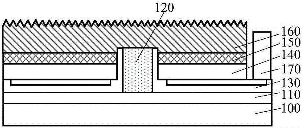
[0034] figure 1It is a structural schematic diagram of an LED chip, and the LED chip includes: a bonding substrate 100; a bonding layer 110 located on the bonding substrate 100; a first electrode layer 120 located on the bonding layer 110; 120 sidewall, and the insulating layer 130 on the bonding layer 110; the first semiconductor layer 140 on the insulating layer 130, the active layer 150 on the first semiconductor layer 140, the first electrode layer 120 and the first The insulating layer 130 on the sidewall of the electrode layer 120 runs through the first semiconductor layer 140 and the active layer 150; the second semiconductor layer 160 located on the active layer 150, the insulating layer 130 and the first electrode layer 120; The second semiconductor layer 160 , the active layer 150 and the second electrode layer 170 of the first electrode...


PUM


Abstract

The present invention provides a LED chip and a formation method thereof. The method comprises: providing a first substrate which is provided with a front end structure consisting of a first semiconductor layer, an active layer and a second semiconductor layer from up to down, wherein the front structure has a zone 1 and a zone 2; forming a groove at the zone 1, wherein the groove penetrates the second semiconductor layer and the active layer; forming a connection conducting layer at the zone 1 around the groove and at the surface of the top of the second semiconductor layer; forming an insulation layer covering the connection conducting layer and the side wall of the groove and exposing the first semiconductor layer at the bottom of the groove and the surface of the top of the second semiconductor layer of the zone 2; performing the bonding processing to allow the insulation layer, the first semiconductor layer at the bottom of the groove and the second semiconductor layer of the zone 2 to combine with a second substrate through a bonding body; removing the first substrate; etching the front end structures of the zone 1 and the part of the zone 2 to respectively correspondingly expose part of the bonding body and the connection conducting layer; and forming an electrode layer at the surfaces of the connection conducting layer and the bonding body. The LED chip formation method can reduce the chip packaging complexity on a LED chip board.

Description

technical field [0001] The invention relates to the field of semiconductor manufacturing, in particular to an LED chip and a forming method thereof. Background technique [0002] A light emitting diode (Light Emitting Diode, referred to as LED) is a semiconductor light emitting device. Light-emitting diodes have photoelectric properties such as low energy consumption, small size, long life, good stability, fast response, and stable emission wavelength. At present, light-emitting diodes are widely used in the fields of lighting, home appliances, display screens, and indicator lights. [0003] The structure of the LED chip includes a positive structure, a flip structure and a vertical structure. [0004] The light emitted by the active area of ​​the front-mounted structure LED exits through the P-type GaN layer and the transparent electrode. However, there are two obvious disadvantages in front-mount LEDs: the current flows laterally through the N-type GaN layer, resulting ...

Claims


Application Information

Patent Timeline
Patent Type & Authority Applications(China)
IPC IPC(8): H01L33/00H01L33/38H01L33/64
CPCH01L33/0093H01L33/382H01L33/641
Inventor 童玲徐慧文
Owner ENRAYTEK OPTOELECTRONICS
Why Eureka
Try Eureka