Display substrate, manufacturing method thereof, and display device

A technology for displaying substrates and manufacturing methods, which is applied in semiconductor/solid-state device manufacturing, instruments, semiconductor devices, etc. It can solve problems such as strength reduction, brittleness and hardening, and easy falling off, so as to prevent water vapor from contacting the metal layer, high hardness and Effects of aging resistance, reliability and safety improvement

Inactive Publication Date: 2019-10-15
BOE TECH GRP CO LTD +1
View PDF2 Cites 0 Cited by
  • Summary
  • Abstract
  • Description
  • Claims
  • Application Information

AI Technical Summary

Problems solved by technology

However, UV glue is easy to fall off at high temperature, and it will become brittle and hard when it is cold, and its strength will decrease. Therefore, it is not suitable for the protection of via holes.

Method used


Image

  • Display substrate, manufacturing method thereof, and display device
  • Display substrate, manufacturing method thereof, and display device
  • Display substrate, manufacturing method thereof, and display device

Examples


Embodiment 1

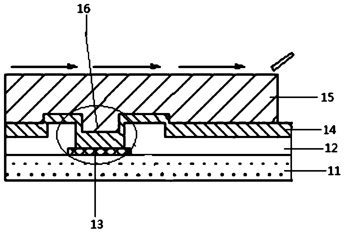
[0053] form the drain on the substrate,

[0054] forming an insulating layer pattern including via holes on the drain;

[0055] A pixel electrode pattern is formed on the insulating layer pattern, and the pixel electrode pattern is connected to the drain of the display substrate through the via hole.

[0056] A water-absorbing thermosetting resin layer covering at least a part of the pixel electrode pattern is formed.

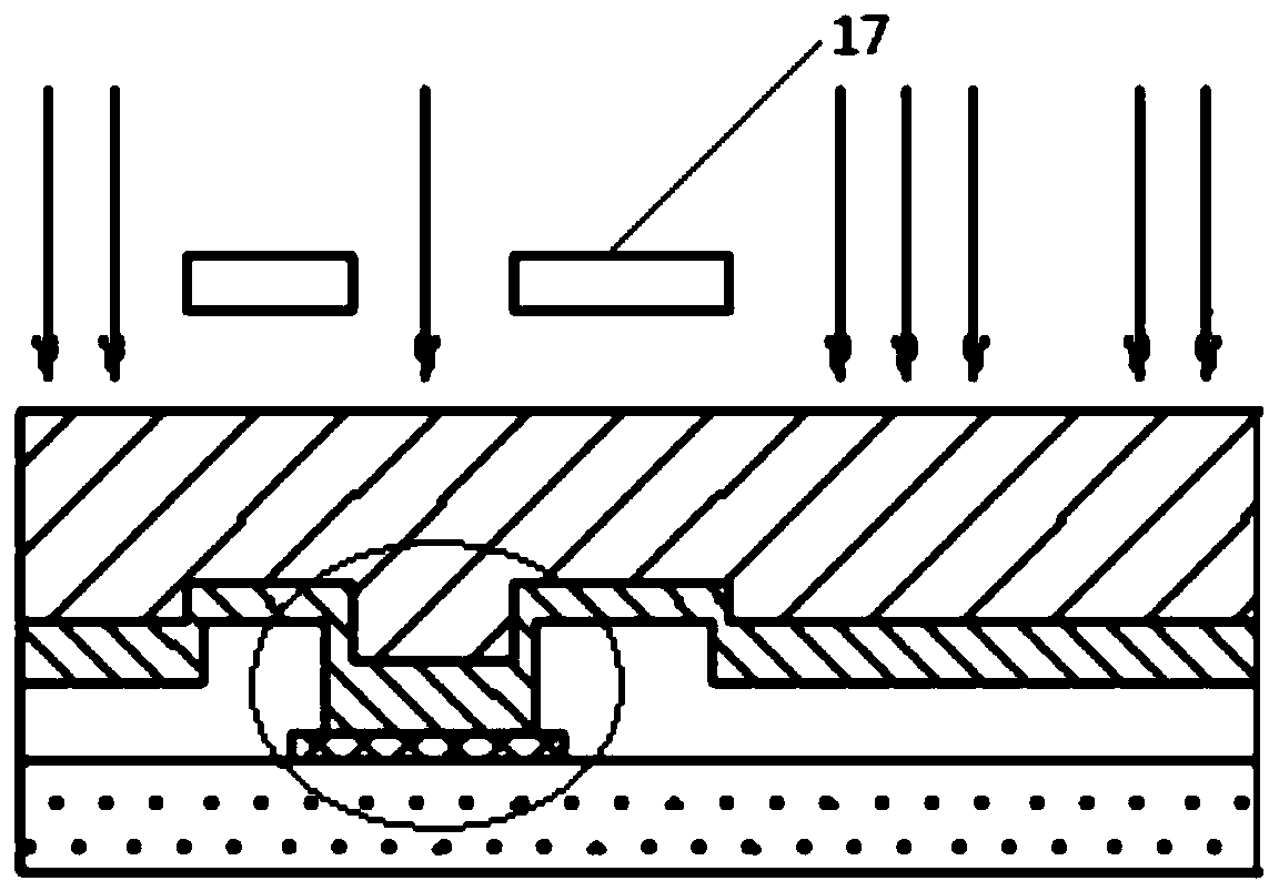
[0057] Specifically, the acrylic resin containing hydroxyl groups can be coated on the surface of the display substrate on which the pixel electrode pattern is formed, and after curing, it is etched to 600 nm, so that the surface of the display substrate is completely covered with the polyacrylic resin layer.

[0058] The processed display substrate is used in a display device, and it is continuously lit and operated for 240 hours in an environment of 60°C and 90% relative humidity. During the test, there is no abnormality in the screen display, and the produc...

Embodiment 2

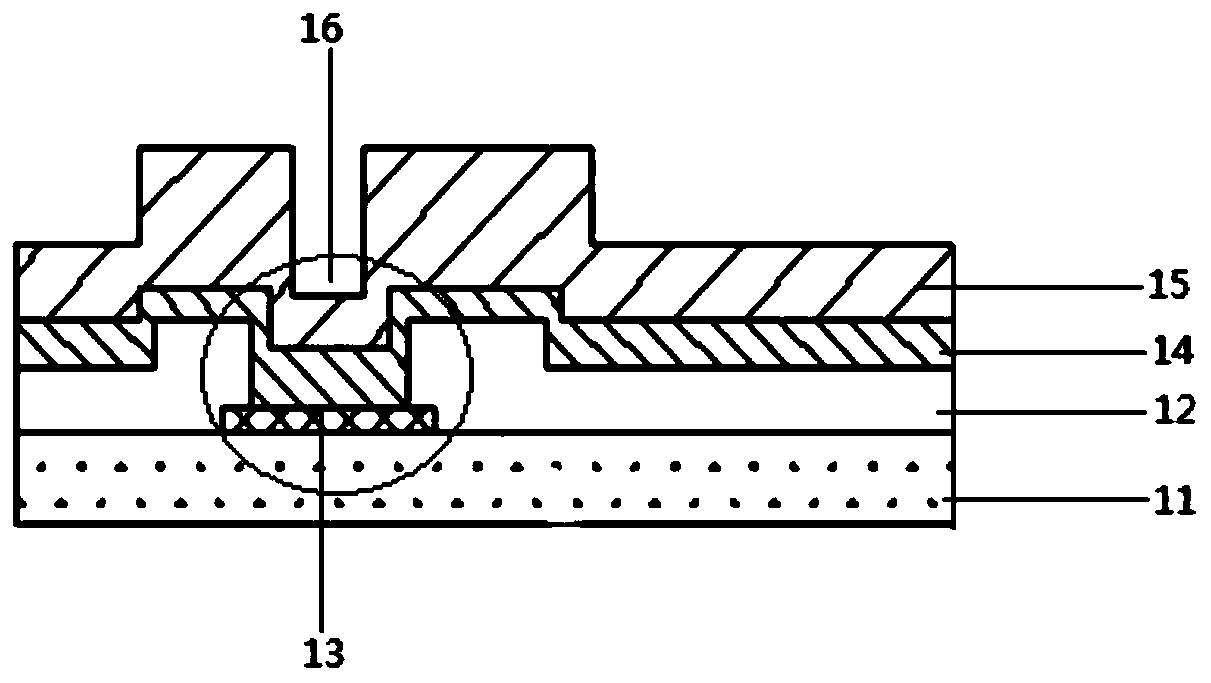
[0060] like Figure 4 As shown, the pattern of the first electrode 21 is formed on the substrate 10 through a patterning process.

[0061] A metal layer 22 is formed on the surface of the substrate on which the pattern of the first electrode 21 is formed; the metal layer 22 is electrically connected to the pattern of the first electrode 21 .

[0062] The insulating layer 12 is formed on the surface of the substrate on which the metal layer 22 is formed.

[0063] Via holes 16 are formed on the surface of the insulating layer 12 through a patterning process.

[0064] The pattern of the second electrode 23 is formed on the insulating layer pattern on which the via hole 16 is formed by a patterning process. Wherein, the second electrode 23 is electrically connected to the metal layer 22 through the via hole 16 .

[0065] Coating the acrylic resin containing hydroxyl groups on the surface of the display substrate on which the second electrode pattern is formed, and after curing,...


PUM

PropertyMeasurementUnit
thicknessaaaaaaaaaa

Abstract

The invention relates to the field of displaying. A manufacture method of a display substrate comprises: forming a metal layer pattern; forming an absorbent thermosetting resin layer covering at least part of the metal layer pattern. Resin used herein is water-absorbent, can absorb trace moisture brought by the environment, has high hardness and aging resistance, is effective in preventing water from contacting a metal layer, especially a metal layer with via holes, and the reliability and safety of a display device in severe environments, such as high temperature and high humidity, are effectively improved.

Description

technical field [0001] The invention relates to the display field, in particular to a display substrate, a manufacturing method thereof and a display device. Background technique [0002] As a flat panel display device, thin film transistor-liquid crystal display has the characteristics of small size, low function, no radiation, and relatively low manufacturing cost, so it is more and more used in the field of high-performance display. [0003] The display panel of the thin film transistor-liquid crystal display includes an array substrate and a color filter substrate. In the manufacturing process of the display panel, wiring design is a very important content. Wherein, it is necessary to realize electrical connection between film layers of different layers such as data lines, gate lines, and common electrode lines through via holes. [0004] Vias are a common design used for bonding metal wires in liquid crystal display devices. Due to the metal heterogeneity and design d...

Claims


Application Information

Patent Timeline
Patent Type & Authority Patents(China)
IPC IPC(8): H01L21/77H01L27/12G02F1/1333
Inventor 刘弘李阳恒袁旭晨张乐
Owner BOE TECH GRP CO LTD
Why Eureka
Try Eureka