Package structure of semiconductor light-emitting chip with airtight window free of silica gel

A light-emitting chip and packaging structure technology, which is applied in the field of lighting, can solve the problems of poor airtightness, increased cost investment, and high equipment requirements, so as to reduce equipment investment, high yield rate, and process simple and reliable effect

Active Publication Date: 2017-02-22
深圳市五矿发光材料有限公司
View PDF3 Cites 17 Cited by
  • Summary
  • Abstract
  • Description
  • Claims
  • Application Information

AI Technical Summary

Problems solved by technology

[0003] For this reason, packaging technology of ceramics, metal and glass has appeared on the market, but when applying the above packaging technology, multiple welding parts and parallel seam welding technology are required. The packaging process is cumbersome and requires high equipment, which increases the cost. input, in addition, the hermeticity after encapsulation is not well guaranteed

Method used


Image

  • Package structure of semiconductor light-emitting chip with airtight window free of silica gel
  • Package structure of semiconductor light-emitting chip with airtight window free of silica gel
  • Package structure of semiconductor light-emitting chip with airtight window free of silica gel

Examples


Embodiment Construction

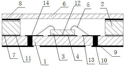
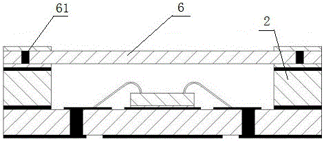
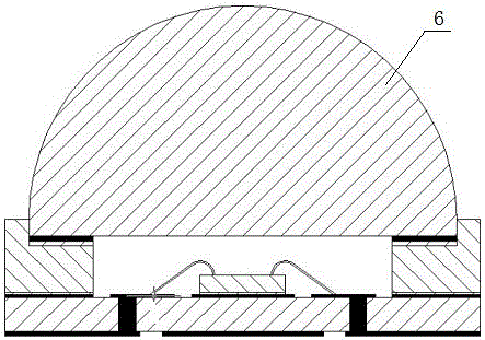
[0031] In order to make the purpose, technical solutions and advantages of the embodiments of the present invention clearer, the technical solutions in the embodiments of the present invention will be clearly and completely described below in conjunction with the drawings in the embodiments of the present invention. Obviously, the described embodiments It is a part of embodiments of the present invention, but not all embodiments. Based on the embodiments of the present invention, all other embodiments obtained by persons of ordinary skill in the art without making creative efforts belong to the protection scope of the present invention.

[0032] It should be noted that, in the case of no conflict, the embodiments in the present application and the technical features in the embodiments can be combined with each other. For example, the first solder pre-set or the second pre-solder described below can be replaced by solder, and the die-bonding material can be replaced by pre-sold...


PUM

PropertyMeasurementUnit
wavelengthaaaaaaaaaa

Abstract

The invention provides a package structure of a semiconductor light-emitting chip with an airtight window free of silica gel and relates to the technical field of illumination. A package device comprises a ceramic body, wherein the ceramic body is a plate-like object; a metal frame placement area, a chip placement area and a gold wire welding area are arranged on the surface of the ceramic body; the metal frame placement area, the chip placement area and the gold wire welding area are coated with a weldable material capable of carrying out welding; the surface of the metal frame is coated with the weldable material; a die bonding material is arranged between the semiconductor light-emitting chip and the ceramic body; a gold wire is arranged in the gold wire welding area; a first preset soldering lug is arranged between the ceramic body and the metal frame; a second preset soldering lug is arranged between the metal frame and glass; and the melting point of the second preset soldering lug is lower than that of the first preset soldering lug. According to the package structure, input of the cost is greatly reduced; the packaging process is simple; the air tightness and the reliability are further improved; and furthermore, the luminous flux and the luminous power can be improved.

Description

technical field [0001] The invention relates to the field of lighting technology, in particular to a package structure of a semiconductor light-emitting chip with a window airtight and without silica gel. Background technique [0002] At present, the packaging of light-emitting chips mostly uses organic materials such as silica gel and epoxy resin to seal and protect the chips. These materials have good transparency, are easy to operate, and can increase the amount of light output, but they have poor UV resistance and are prone to aging and deterioration in ultraviolet environments. . The traditional semiconductor light-emitting chip packaging structure packaging method uses silica gel as the packaging material. When the packaging is exposed to ultraviolet light, it is easy to crack and age, and it is easy to die and cause device failure. Therefore, organic materials are not conducive to packaging ultraviolet LED devices and are not suitable for the use of organic materials....

Claims


Application Information

Patent Timeline
Patent Type & Authority Applications(China)
IPC IPC(8): H01L23/31H01L23/488H01L23/528
CPCH01L23/31H01L23/488H01L23/528H01L2224/16225H01L2224/48091H01L2224/48227H01L2224/73265H01L2924/00014
Inventor 詹勋县
Owner 深圳市五矿发光材料有限公司
Why Eureka
Try Eureka