
Manufacturing method of light-emitting diode
A technology of light-emitting diodes and manufacturing methods, which is applied in the direction of electrical components, circuits, semiconductor devices, etc., can solve the problems of easy damage and low appearance yield of Micro LED, and achieve the effect of improving the appearance yield
- Summary
- Abstract
- Description
- Claims
- Application Information
AI Technical Summary
Problems solved by technology
Method used
Image

Examples
Embodiment Construction
[0040] In order to make the object, technical solution and advantages of the present invention clearer, the implementation manner of the present invention will be further described in detail below in conjunction with the accompanying drawings.
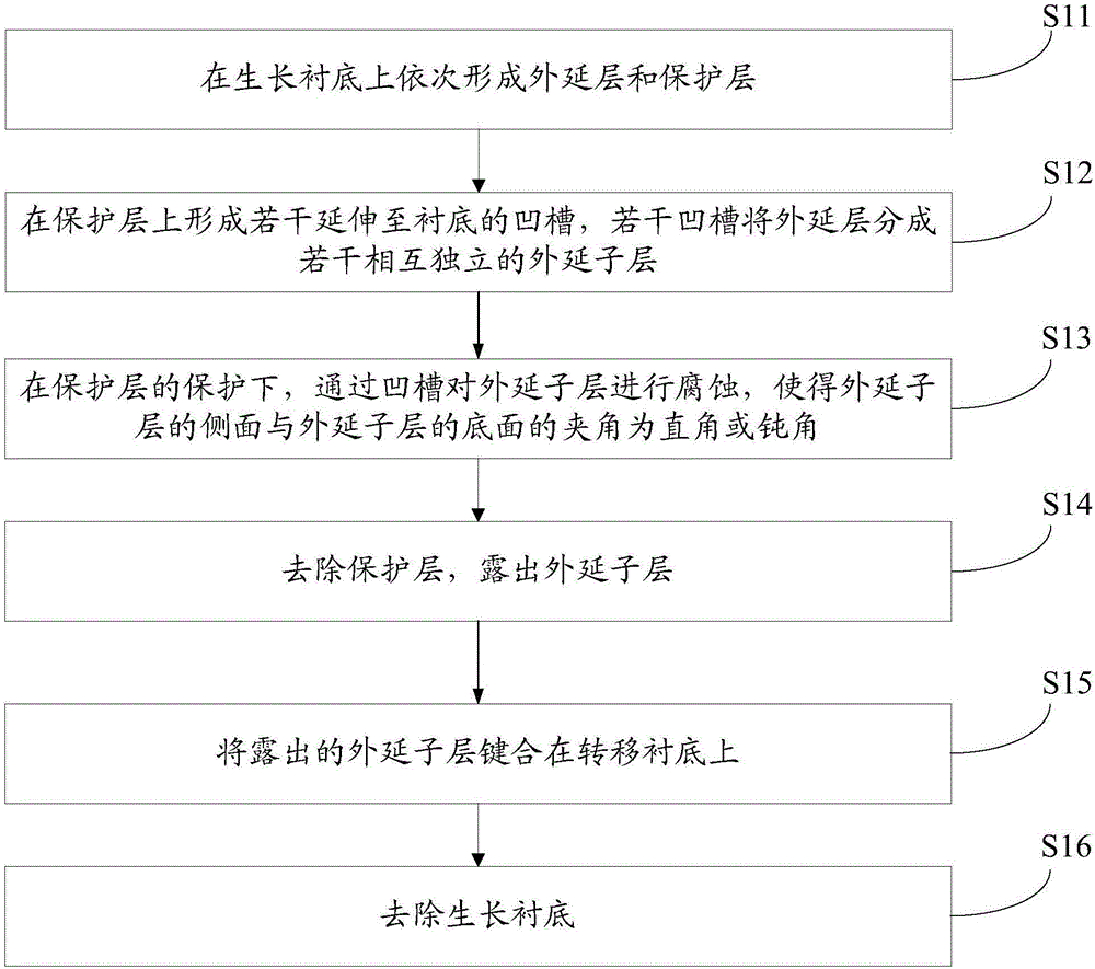
[0041] The embodiment of the present invention provides a method for manufacturing a light emitting diode, figure 1 It is a flowchart of a method for manufacturing a light-emitting diode provided by an embodiment of the present invention, such as figure 1 As shown, the method includes:
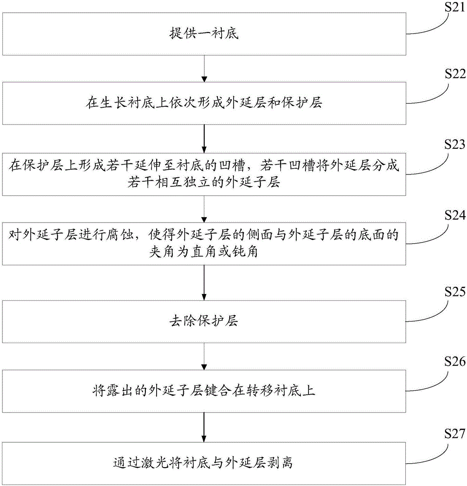
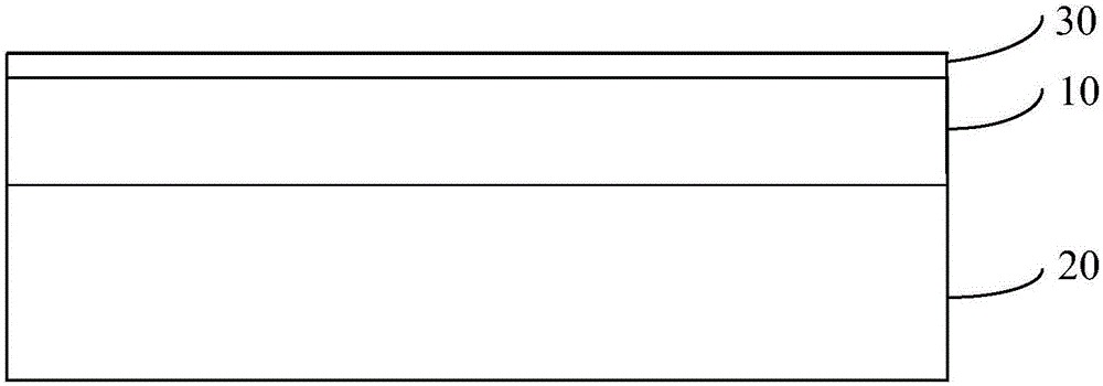
[0042] S11: sequentially forming an epitaxial layer and a protective layer on the growth substrate.
[0043] S12: Forming a plurality of grooves extending to the substrate on the protection layer, the plurality of grooves dividing the epitaxial layer into a plurality of independent epitaxial sub-layers.
[0044] S13: Under the protection of the protective layer, the epitaxial sublayer is etched through the groove, so that the angle between the side s...
PUM
 Abstract
Description
Claims
Application Information