

Processing method of chip after laser cutting
A processing method and chip technology, which is applied in the manufacture of electrical components, circuits, semiconductors/solid-state devices, etc., can solve problems such as adhesion to the surface of chips, easy generation of crack fragments, delamination, and low utilization of chips, so as to achieve improvement in Chip surface, improve appearance yield, improve wettability effect
Active Publication Date: 2020-05-22
XIAMEN SANAN INTEGRATED CIRCUIT
View PDF10 Cites 0 Cited by
- Summary
- Abstract
- Description
- Claims
- Application Information
AI Technical Summary
Problems solved by technology
The traditional cutting methods include diamond slitting cutting and wheel cutting. The traditional cutting methods have the following problems: 1. Wide cutting groove (30-100um), low utilization rate of wafers; 2. Cracks, fragments, and delamination are easy to occur; 3. , Tool consumption is fast, a large amount of deionized water needs to be consumed, which increases costs, etc.
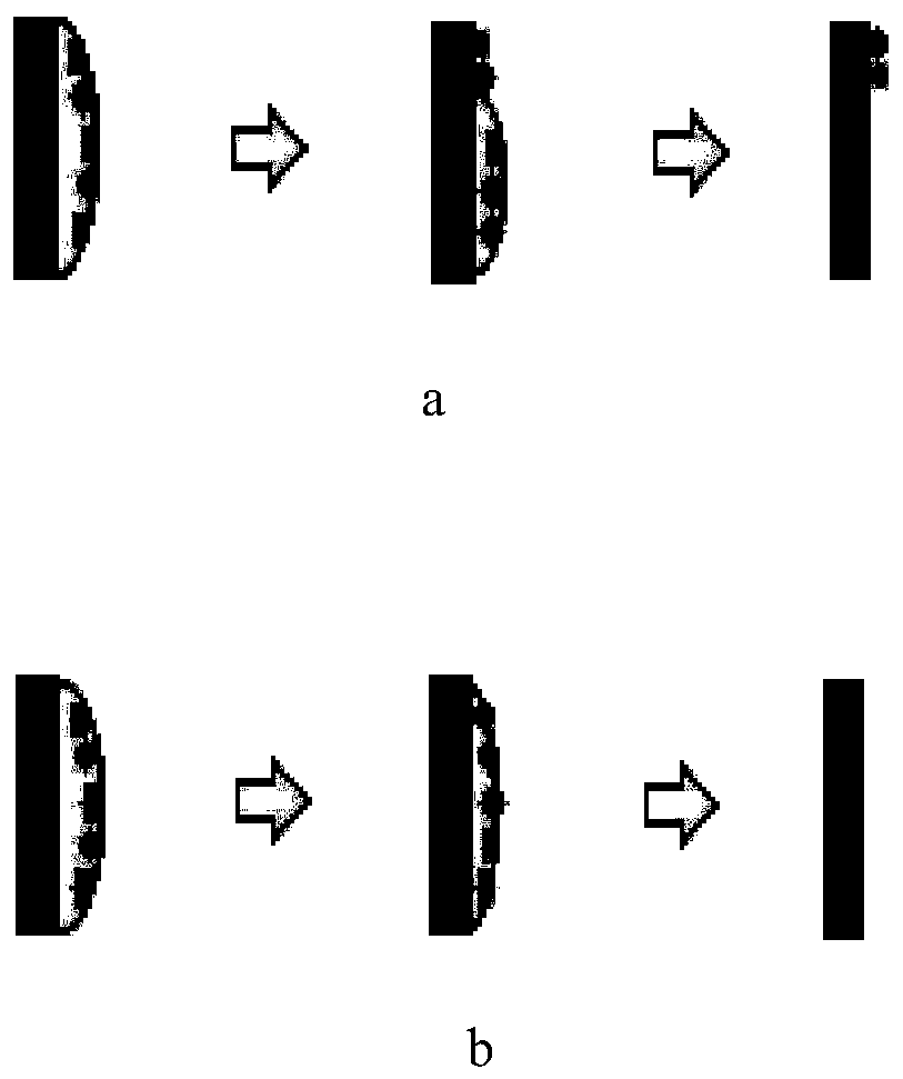
However, the conventional method has the following problems: 1) some amalgam particles will be suspended in the etching solution during the etching process, and some will stick back to the chip surface; 2) there will be residual etching solution on the surface when the wafer leaves the etching solution after etching , there are some burnt particles in the residual etching solution. During the transmission to the cleaning process, due to the surface tension, the etchant will quickly concentrate on the lower half of the chip and be removed in the subsequent cleaning process, resulting in the burnt particles in the upper part. Particles adhere to the surface of the chip and cannot be removed by subsequent cleaning
The above problems cause a loss of appearance yield that cannot be ignored
Method used
View moreImage
Smart ImageViewing Examples

Examples
Embodiment 1
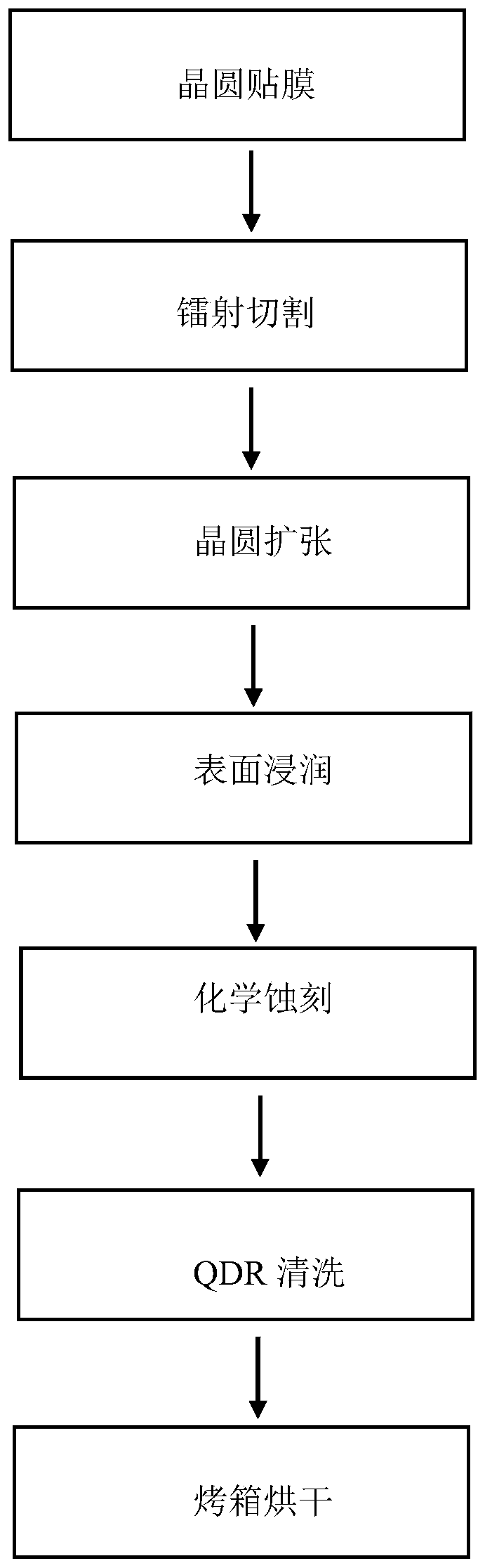
[0036] Using the above method, a GaAs wafer with a thickness of 90um is cut with a 4W power UV laser, soaked in a surfactant solution for 100s after cutting, then soaked in an etching solution for 40s, and then transferred to a quick-discharge rinse tank and rinsed with DI water 10min, after cleaning, bake in a 55°C oven for 30min. Among them, the surfactant is: water 83.8%, polyethylene glycol 4.1%, polyethylene glycol octyl phenyl ether 3.2%; the etching solution is a mixed solution of ammonia water: hydrogen peroxide: water = 1:1:10.
Login to View More PUM
 Abstract
The invention discloses a processing method of a chip after laser cutting. The method comprises the steps of: performing laser cutting and wafer expanding processing on a chip to form a plurality of independent chips, soaking the chips in a surfactant solution for a period of time, removing the chips from the surfactant solution, soaking the chips in an etching solution, etching a burning melt onthe edges of the chips through the etching solution, cleaning the etched chips, removing the residual etching solution on the surfaces of the etched chips, and drying the cleaned chips. After the chipis subjected to laser cutting and before the chip is etched, the surface active agent is adopted to improve the wettability of the surface of the chip, so that on one hand, burnt and melted particlesare prevented from being stuck back to the surface of the chip in the etching process; and on the other hand, the burnt and melted material particles are prevented from being attached to the surfaceof the chip in the process of conveying the etched chip to the cleaning link, so that the condition that the burnt and melted material particles stay on the surface of the chip in the subsequent etching and cleaning process is improved, and the appearance yield of products is improved.
Description
technical field [0001] The invention relates to the technical field of chip cutting, in particular to a processing method for chips after laser cutting. Background technique [0002] In recent years, III-V semiconductors have become more and more widely used. In order to greatly save costs and improve production efficiency, integrated circuit chips are often deposited on wafers in mass production, and then divided into individual units, and finally packaged and soldering. Wafer dicing technology has an important impact on improving yield and packaging efficiency. The traditional cutting methods include diamond slitting cutting and wheel cutting. The traditional cutting methods have the following problems: 1. Wide cutting groove (30-100um), low utilization rate of wafers; 2. Cracks, fragments, and delamination are easy to occur; 3. , Tool consumption is fast, need to consume a lot of deionized water, increase the cost and so on. Laser cutting technology integrates optics, ...
Claims
Login to View More Application Information
Patent Timeline
 Patent Type & Authority Applications(China)
IPC IPC(8): H01L21/02H01L21/304
CPCH01L21/02057H01L21/3043
Inventor 王伟林科闯伍燕辉陈军李华群许章伟
Owner XIAMEN SANAN INTEGRATED CIRCUIT