Semiconductor module

一种半导体、导体层的技术,应用在半导体器件、半导体/固态器件零部件、电固体器件等方向

Active Publication Date: 2017-02-22
SHINDENGEN ELECTRIC MFG CO LTD
View PDF7 Cites 12 Cited by
  • Summary
  • Abstract
  • Description
  • Claims
  • Application Information

AI Technical Summary

Problems solved by technology

The problem described is a significant one in the use of stacked high heat generating device structures

Method used


Image

  • Semiconductor module
  • Semiconductor module
  • Semiconductor module

Examples


no. 1 Embodiment approach

[0050] [constitute]

[0051] Next, a first embodiment of the semiconductor module according to the present invention will be described with reference to the drawings.

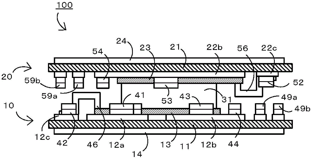
[0052] Such as figure 1 As shown, the semiconductor module 100 of this embodiment includes: a first member 10 , a second member 20 , and a conductor post 31 extending in the vertical direction between the first member 10 and the second member 20 . In this embodiment, the first insulating substrate 11 of the first member 10 and the second insulating substrate 21 of the second member 20 are mounted in parallel. In this embodiment, the extended surfaces of the first insulating substrate 11 and the second insulating substrate 21 ( figure 1 The extension plane towards the left and right direction) is called the horizontal plane; in the direction perpendicular to the horizontal plane (ie figure 1 The up and down direction) is called the up and down direction.

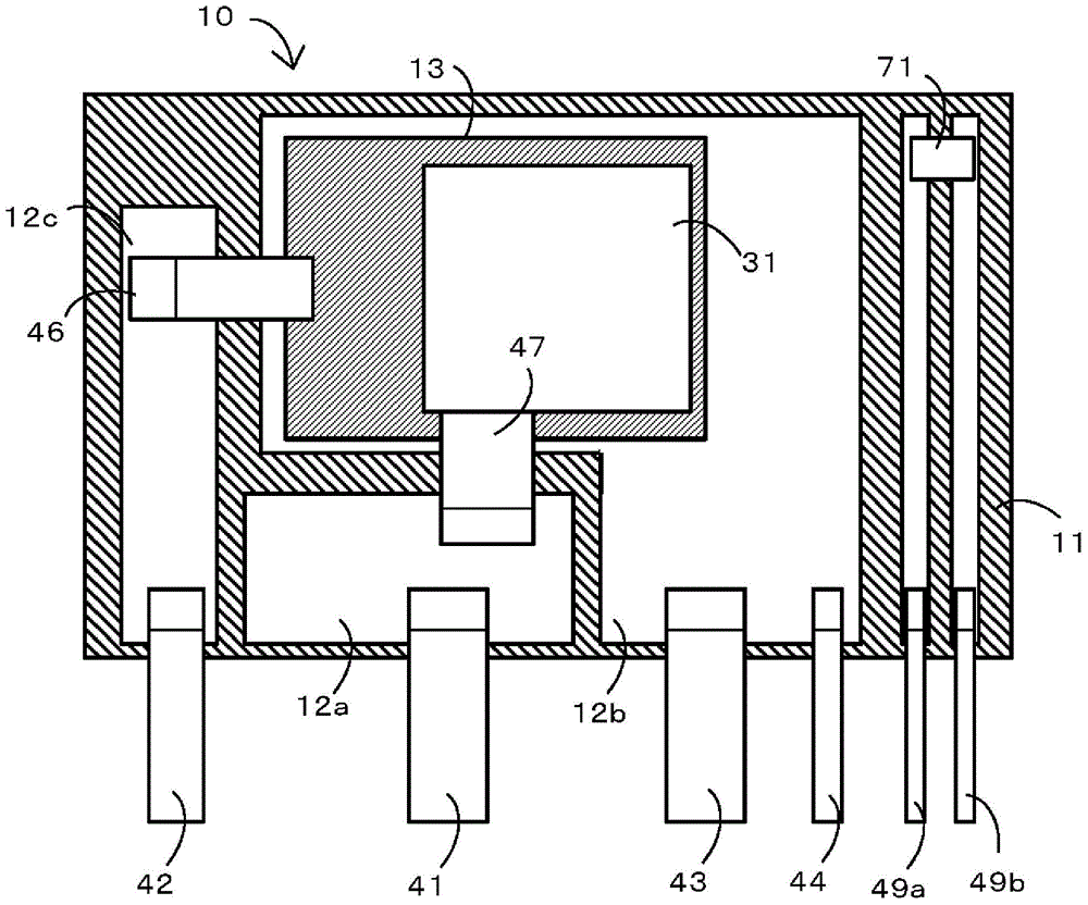
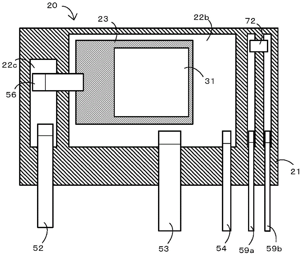
[0053] Such as figure 2 As shown, the first mem...

no. 2 Embodiment approach

[0081] Next, a second embodiment according to the present invention will be described.

[0082] Such as Figure 7 As shown, the second embodiment relates to an electronic device including the semiconductor module 100 described in the first embodiment and a heat sink 200 provided with a concave portion 210 into which the semiconductor module 100 is inserted. The size of the recess 210 is consistent with the size of the semiconductor module 100 . Therefore, as long as the semiconductor module 100 is inserted into the concave portion 210 , the semiconductor module 100 is fixed to the heat sink 200 .

[0083] In the second embodiment, other configurations are slightly the same as those in the first embodiment. In the second embodiment, a detailed description of the same parts as those in the first embodiment will be omitted.

[0084] The inside of the concave portion 210 of the cooling plate 200 may also be coated with a lubricant made of silicon grease or the like, and the sem...


PUM


Abstract

A semiconductor module (100) having: a first member (10); a second member (20); a conductor column (31) extending in the vertical direction, between the first member (10) and the second member (20); and a sealing resin (80) covering a first conductor layer (12) and first power device (13) in the first member (10), a second conductor layer (22) and second power device (23) in the second member (20), and the conductor column (31). The horizontal positions of the first power device (13) and the second power device (23) are displaced, the second conductor layer (22) is not provided in the vertical direction of a first connection section (46) connected to the first power device (13), and the first conductor layer (12) is not provided in the vertical direction of a second connection section (56) for the second member (20) and connected to the second power device (23).

Description

technical field [0001] The present invention relates to a semiconductor module. Background technique [0002] There is known a semiconductor module employing a stacked device structure. As an example of the conventional semiconductor module, International Publication No. 2014-132397 can be cited. The International Publication No. 2014-132397 discloses the following feature: In order to prevent heat generation of the semiconductor module, a structure in which a switching element with a generally high heat generation and a rectification element with a general low heat generation are installed opposite to each other is adopted. [0003] As for the structure, in recent years, a structure in which high heat-generating devices are stacked has been attempted. When stacking the high heat-generating devices 313, 323, as Figure 8 As shown, when the 313, 323 are simply stacked, the heat of the two high-heating 313, 323 overlaps together, and the entire semiconductor module generates...

Claims


Application Information

Patent Timeline
Patent Type & Authority Applications(China)
IPC IPC(8): H01L25/07H01L23/28H01L23/29H01L25/18
CPCH01L25/071H01L25/074H01L2224/40225H01L23/49537H01L23/3142H01L23/49568H01L23/49562H01L23/3675
Inventor 池田康亮
Owner SHINDENGEN ELECTRIC MFG CO LTD
Why Eureka
Try Eureka