

Wave absorbing body structure
A wave absorber and honeycomb structure technology, which is applied in the field of wave absorbers, can solve the problems of high material density and unsatisfactory low surface density, and achieve the effects of reduced thickness, good wave absorption effect, and improved wave absorption performance
- Summary
- Abstract
- Description
- Claims
- Application Information
AI Technical Summary
Problems solved by technology
Method used
Image

Examples
Embodiment 1
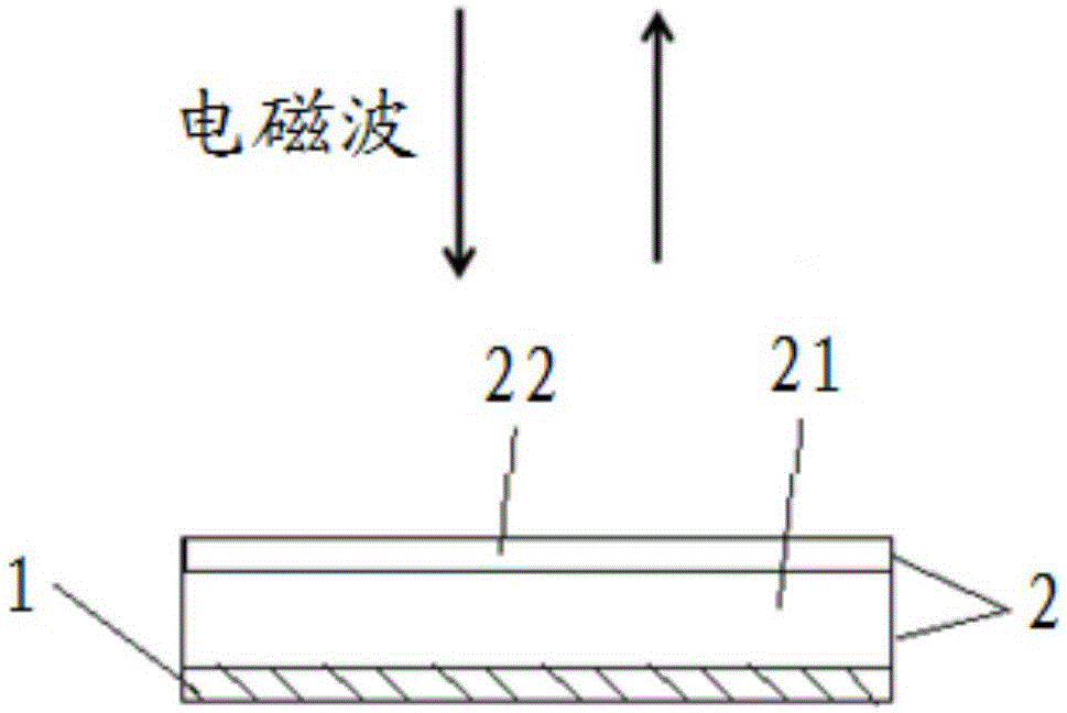
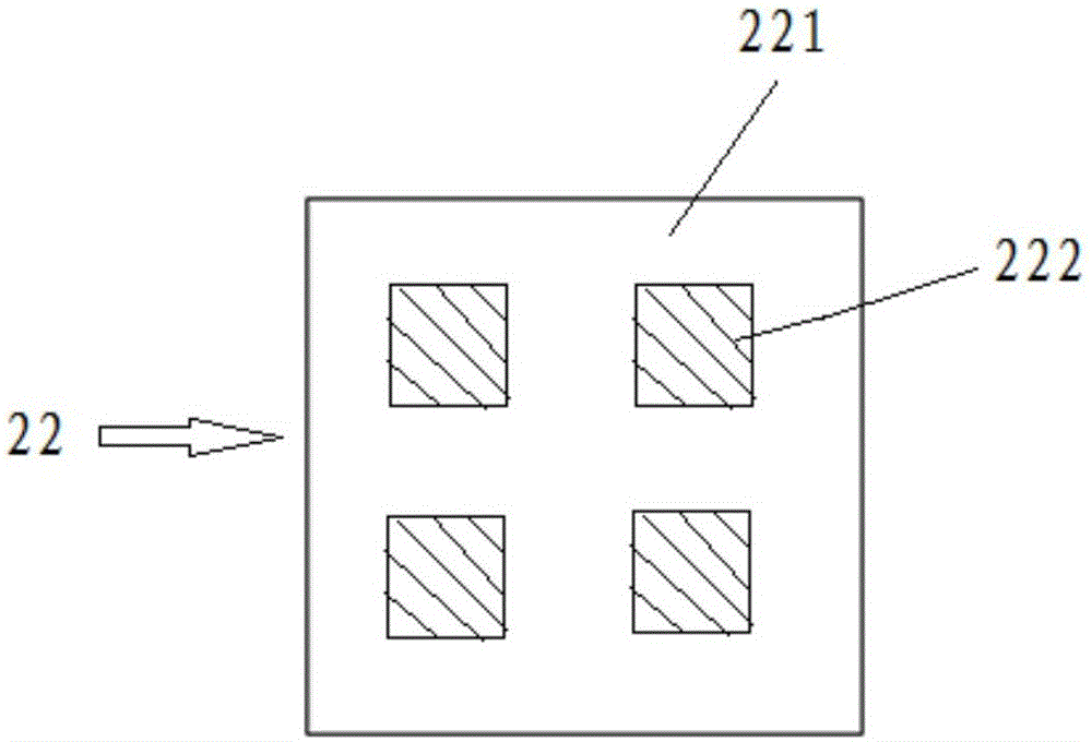
[0043] Such as figure 1As shown, a absorber structure includes a metal base plate 1 and a layer of electrical loss body 2 covered on one surface of the metal base plate 1. The electrical loss body 2 includes a honeycomb layer 21 and a resistor superimposed on a surface of the honeycomb layer 21. sheet layer 22, and the other surface of the honeycomb layer 21 is in close contact with the metal bottom plate 1. The metal bottom plate 1 is a copper bottom plate, and the honeycomb layer 21 includes a polymer resin sheet and a honeycomb structure distributed on the polymer resin sheet. The thickness of the honeycomb layer 21 is 100 mm. figure 2 is a top view of the resistance sheet layer 22, such as figure 2 As shown, the resistor sheet 22 includes a dielectric substrate 221 located below the resistor sheet and four resistor blocks 222 on the surface of the dielectric substrate 221, the dielectric substrate 221 provides a supporting surface for the four resistor blocks 222, wher...
Embodiment 2
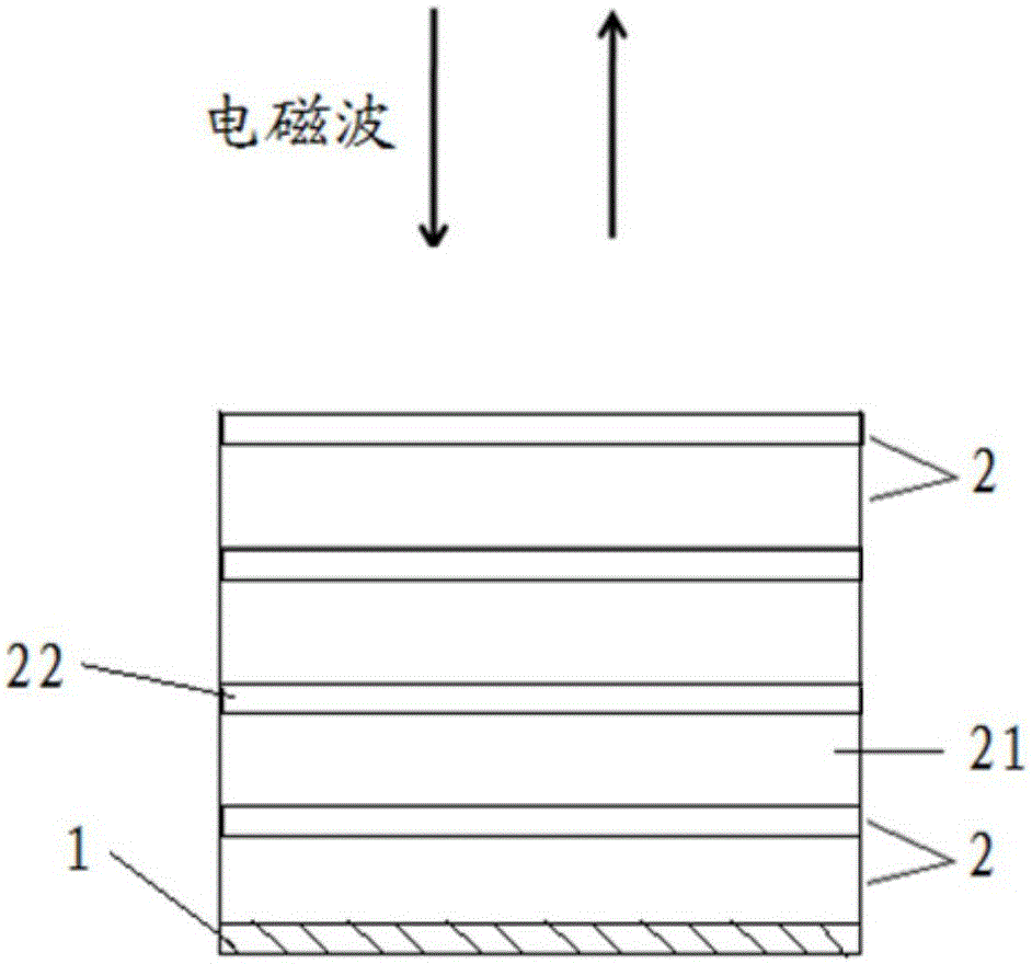
[0045] Such as image 3 As shown, a absorber structure includes a metal base plate 1 and 4 layers of electrical loss bodies 2 covered on one surface of the metal base plate 1, each layer of electrical loss body 2 includes a honeycomb layer 21 and a resistor superimposed on the honeycomb layer 21 The sheets 22, 4 layers of honeycomb layers 21 and 4 layers of resistive sheets 22 are formed by stacking each other alternately. The metal bottom plate 1 is an aluminum bottom plate, and the honeycomb layer 21 includes a polymer resin sheet and a honeycomb structure distributed on the polymer resin sheet. The thickness of each layer of honeycomb layer 21 is 50mm. Starting from the metal base plate 1, the 4 layers of resistance sheets include 4, 6, 5, and 7 oval resistance blocks 223 in sequence. The ellipse resistance blocks 223 in each layer of resistance sheets Shaped resistance blocks 223 are randomly arranged, the size of the resistance sheets in different resistance sheet layers...
Embodiment 3
[0047] An absorber structure includes a metal base plate and 4 layers of electrical loss bodies covered on one surface of the metal base plate, each layer of electrical loss body includes a honeycomb layer and a resistance sheet layer superimposed on the honeycomb layer, 4 layers of honeycomb layers and 4 layers The layer resistor sheets are formed by stacking each other alternately. The metal base plate is a silver base plate, and the honeycomb layer includes a polymer resin sheet and a honeycomb structure distributed on the polymer resin sheet. The thickness of each layer of honeycomb layer from the direction close to the metal bottom plate is 1mm, 10mm, 50mm, 30mm, each of the 4 layers of resistance sheet includes 6 triangular resistance blocks, and the triangular resistance blocks in each layer of resistance sheet The sizes are different, but they are all arranged periodically in an array. Each resistance sheet layer includes a dielectric substrate located below the resis...
PUM
 Abstract
Description
Claims
Application Information