Semiconductor component image test device and its test equipment

A technology of testing equipment and testing equipment, which is applied in the direction of semiconductor/solid-state device testing/measurement, measuring equipment, instruments, etc., and can solve problems such as inability to achieve high-speed transmission frequency, inability to meet high-efficiency semiconductor component test specifications, narrow bandwidth, etc.

Active Publication Date: 2019-12-24
KING YUAN ELECTRONICS
View PDF9 Cites 0 Cited by
  • Summary
  • Abstract
  • Description
  • Claims
  • Application Information

AI Technical Summary

Problems solved by technology

[0003] However, under this test framework, more than two sets of circuit boards, the load board and the DUT board, must be used for power supply requirements and signal transmission. Among them, the bandwidth is relatively narrow and cannot reach high-speed transmission frequency, so it cannot meet the test specifications of high-performance semiconductor components

Method used


Image

  • Semiconductor component image test device and its test equipment
  • Semiconductor component image test device and its test equipment
  • Semiconductor component image test device and its test equipment

Examples


Embodiment Construction

[0034] The above summary and the following detailed description are exemplary in order to further illustrate the scope of the present invention. Other purposes and advantages of the present invention will be described in the subsequent description and illustrations.

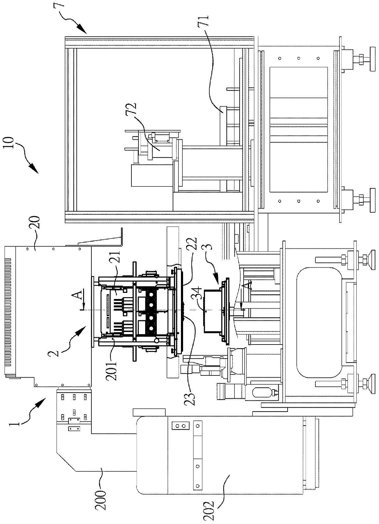
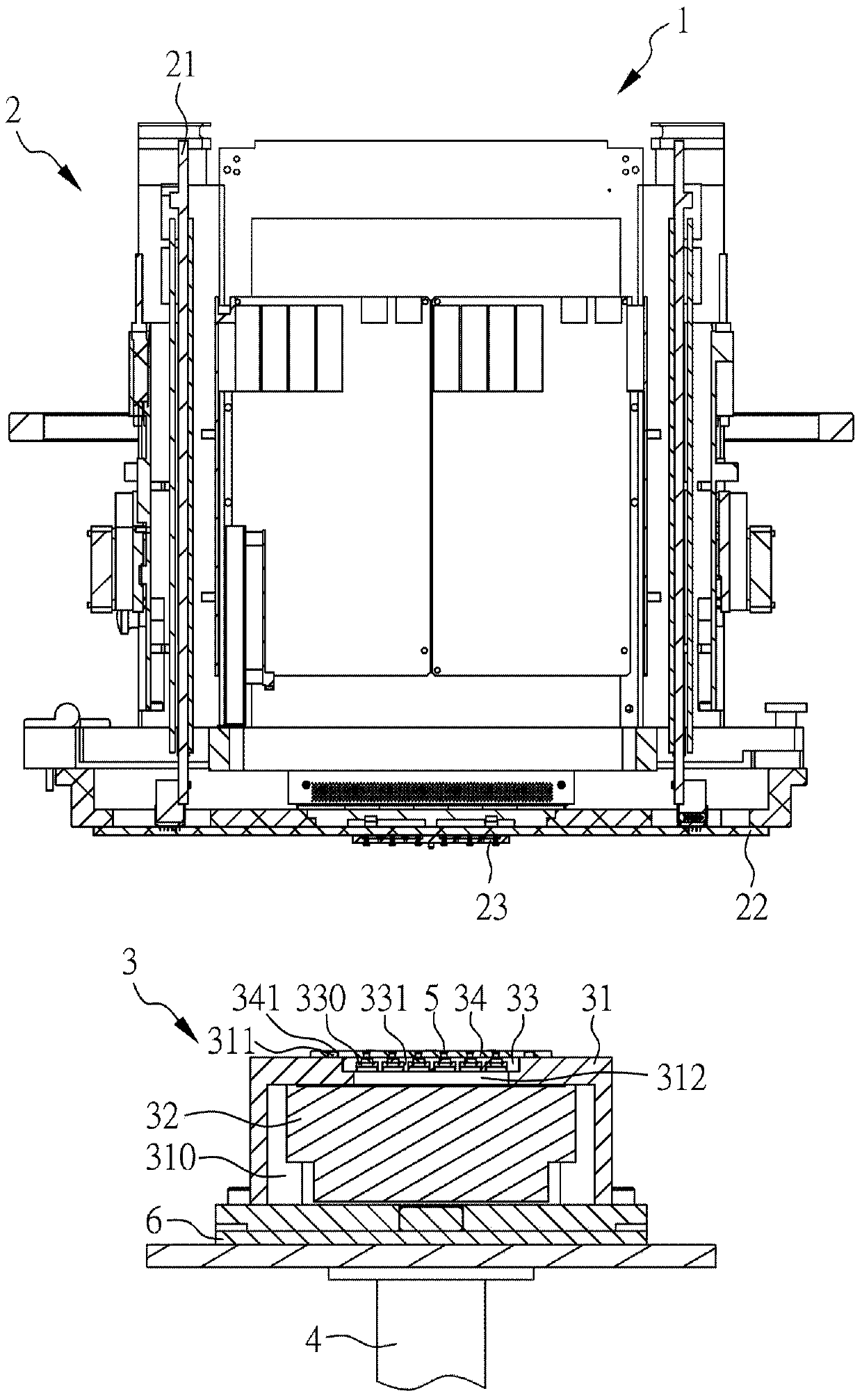
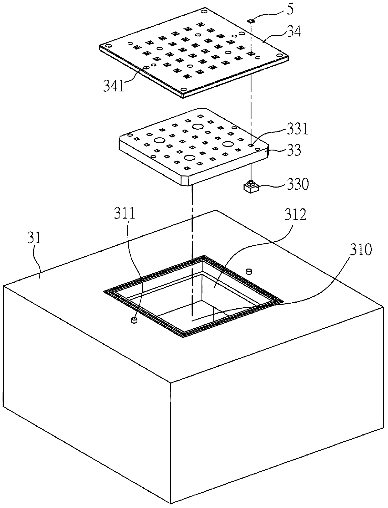
[0035] see figure 1 , is a side view of a semiconductor device image testing device according to a preferred embodiment of the present invention. The figure shows a semiconductor element image test equipment 10, which includes a semiconductor element image test device 1 and a sorting machine 7, wherein the semiconductor element image test device 1 further includes a test circuit module 2 and a mobile light source module 3. In this embodiment, the above-mentioned test circuit module 2, a mobile light source module 3, and the sorting machine 7 have a separate structure, so under the same test structure, it is possible to fine-tune some modules and test other final test logic products to achieve Image test shares...


PUM


Abstract

The invention relates to a semiconductor element image test device and test equipment thereof. The semiconductor element image test device comprises a test circuit module and a movable light source module. The test circuit module is arranged on a main frame connected to a test head, and comprises at least one circuit board, one interface board, and a probe test base fixedly arranged on the interface board. The movable light source module is arranged on an elevating device and comprises a base, a light source supply device, and a lens set carrier plate, on which a plurality of lens are loaded. The elevating device can selectively drive the movable light source module to make the movable light source module contact with or does not contact with the test circuit module, and thus at least half of semiconductor elements in a test carrier plate contacts with or does not contact with the probe test base. Through the setting of modules, the light source supply device and a plurality of optical lens can be conveniently installed, maintained, and picked / placed. At the same time, the test signals can be directly delivered to the image test circuit and test probe, and the signal transmission stability is enhanced.

Description

technical field [0001] The invention relates to a semiconductor element image test device and its test equipment, especially a test device and its test equipment suitable for testing the image characteristics of a semiconductor element. Background technique [0002] With regard to the existing semiconductor device image testing device, the current configuration structure on the market is to set the test light source in a test head located under the machine table, and set a load board, a load board, and a test head on the test head in sequence The test board (DUT board) and a carrier plate for placing semiconductor components, and in the process of image testing, the semiconductor components and the test board are pressed down through a pin tester on a sorter, and the test signal is flattened The cables are fed into the test head for analysis of the vision test results. [0003] However, under this test framework, more than two sets of circuit boards, the load board and the ...

Claims


Application Information

Patent Timeline
Patent Type & Authority Patents(China)
IPC IPC(8): G01N21/84H01L21/66
Inventor 吴国荣梁兴岳
Owner KING YUAN ELECTRONICS
Why Eureka
Try Eureka