
Apparatus for fabricating variable period photonic crystals based on multi-beam interferometry

A technology of multi-beam interference and photonic crystals, which is applied in photolithography exposure devices, microlithography exposure equipment, optics, etc., can solve problems such as difficult adjustment of beam incident angles and complex optical paths, and achieves strong portability and simple operation , the effect of simple structure

Inactive Publication Date: 2018-06-05
XIAMEN UNIV
View PDF2 Cites 0 Cited by
  • Summary
  • Abstract
  • Description
  • Claims
  • Application Information

AI Technical Summary

Problems solved by technology

[0006] The purpose of the present invention is to provide a multi-beam based multi-beam interference lithography system with simple structure, strong operability and large-area variable period for the shortcomings of the existing multi-beam interference lithography system, such as complex optical path and difficult adjustment of beam incident angle. Device for manufacturing variable-period photonic crystals by interferometry

Method used


Image

  • Apparatus for fabricating variable period photonic crystals based on multi-beam interferometry
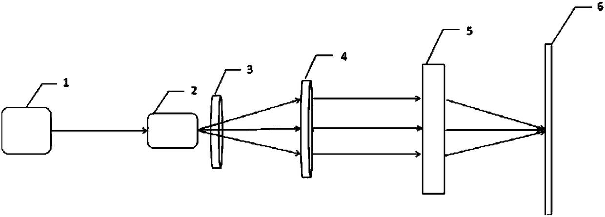
  • Apparatus for fabricating variable period photonic crystals based on multi-beam interferometry
  • Apparatus for fabricating variable period photonic crystals based on multi-beam interferometry

Examples


Embodiment Construction

[0020] The present invention will be described in detail below in conjunction with the accompanying drawings and specific embodiments. However, the following examples are limited to explain the present invention.

[0021] The present invention is a device for manufacturing variable-period photonic crystals based on the multi-beam interference method. When using the device to prepare three-dimensional photonic crystals, it needs to be realized through the following steps:

[0022] Step 1: If figure 1 As shown, the spatial filter 2 is placed in the propagation direction of the laser output from the laser 1, and the light outlet of the spatial filter 2 must be at the focus of the convex lens 4. When the laser beam is expanded by the spatial filter 2, the laser beam will become a A beam of divergent light, because the divergence point of this beam of divergent light is at the focal point of the convex lens 4, it will become a beam of parallel light after passing through the conve...


PUM

PropertyMeasurementUnit
reflectanceaaaaaaaaaa

Abstract

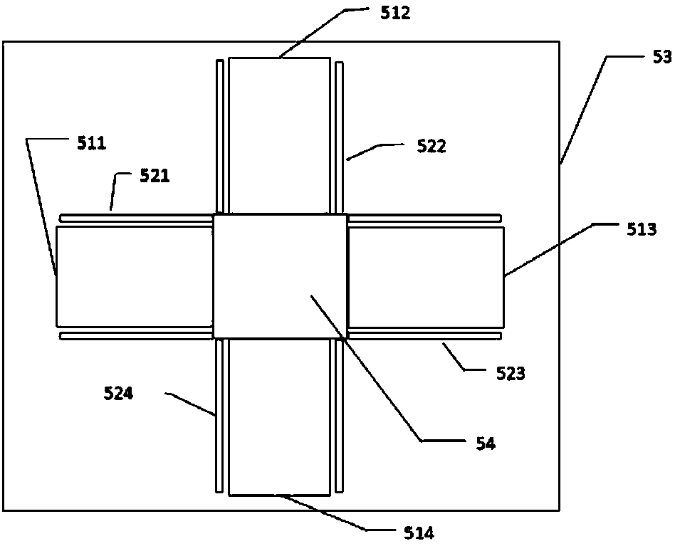
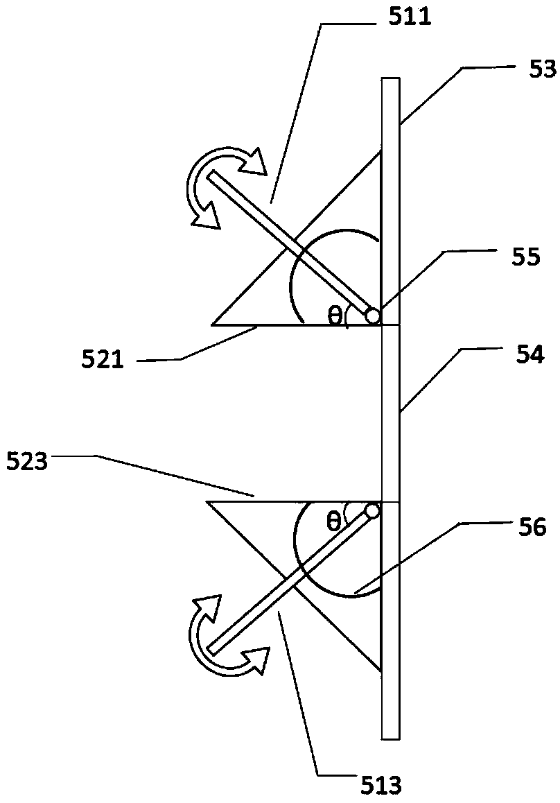
The invention relates to a device for manufacturing a period-variable photonic crystal on the basis of multiple beam interferometry, and relates to photonic crystals. A laser device, a spatial filter, a diaphragm, a convex lens, a multi-beam generation component and a photoresist plate are arranged successively; a light outlet of the spatial filter is arranged in a focus of the convex lens; after the spatial filter carries out beam expanding on laser emitted by the laser device, the laser is changed into a beam of diverging light, the diverging light is changed into a beam of parallel light when passing the convex lens, the beam of parallel light irradiates on the multi-beam generation component along the normal direction, the multi-beam generation component adjusts an optical path of the beam of parallel light to generate multiple coherent light beams, the multiple coherent light beams are overlapped on the photoresist plate, single exposure is carried out on an overlapped interference area of the multiple beams on the photoresist plate, and the period-variable photonic crystal is obtained via development.

Description

technical field [0001] The invention relates to photonic crystals, in particular to a device for manufacturing variable-period photonic crystals based on a multi-beam interference method. Background technique [0002] The precision of laser interference lithography is very high, reaching the micro-nano level. Properly adjusting the angle between the interfering light can even make the period of the micro-nano structure close to half of the laser wavelength. It is a highly operable method. Micro-nano structure preparation technology. [0003] Multi-beam interferometry is commonly used to fabricate photonic crystals. The three-dimensional optical structure can be recorded very conveniently by using the photosensitive properties of the photoresist and the single exposure method. Then through the development process, the prepared structure can be revealed, so as to obtain the desired photonic crystal. [0004] It is well known that the periodic electric potential field genera...

Claims


Application Information

Patent Timeline
Patent Type & Authority Patents(China)
IPC IPC(8): G02B1/00G03F7/20
CPCG02B1/005G03F7/70408
Inventor 何勇林炉庆洪高敏林国强杨志林
Owner XIAMEN UNIV
Learn More