

Multi-light-source interference exposure device
Patent Information
- Authority / Receiving Office
- CN · China
- Patent Type
- Patents(China)
- Current Assignee / Owner
- SHANGHAI MICRO ELECTRONICS EQUIP (GRP) CO LTD
- Publication Date
- 2015-01-21
Smart Images
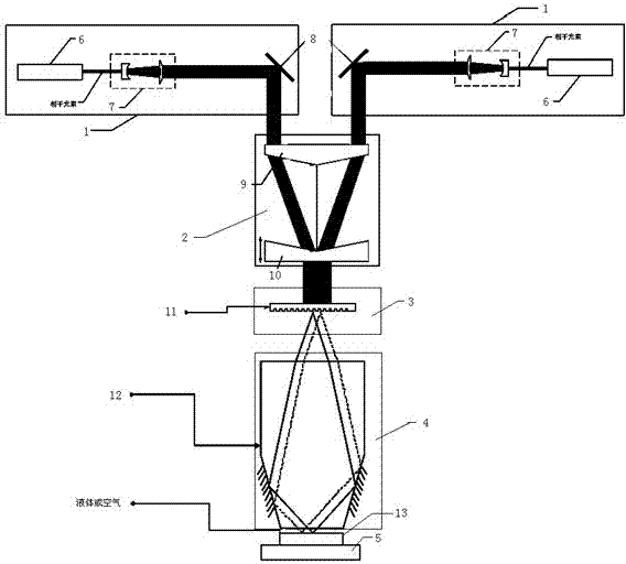
Figure 1 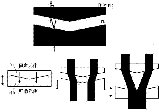
Figure 2 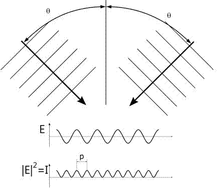
Figure 3
Abstract
Description
technical field
[0001] The invention relates to the technical field of photolithography, in particular to a multi-light source interference exposure device used in photolithography devices. Background technique
[0002] Under the current background that the line width CD in the field of semiconductor manufacturing technology generally enters below 90nm, using the method of optical projection exposure, in order to produce high-resolution periodic patterns within a certain exposure field range, a high-resolution mask is required. It is equipped with a large numerical aperture NA objective lens, resulting in a smaller depth of focus. As the size of the substrate becomes larger (such as 12-inch silicon wafer, sapphire substrate, etc.), it is often difficult to obtain a good substrate flatness, so it is necessary to introduce a complex, high-precision focusing and leveling system to ensure that the exposure surface of the substrate is in the within the depth of focus of the proj...