
Multi-light-source interference exposure device

An interference exposure, multi-light source technology, applied in the field of lithography, can solve the problems of limited exposure light intensity, low laser power, low production efficiency, etc., and achieve the effects of high resolution, improved production efficiency, and simple structure

Active Publication Date: 2013-06-05
SHANGHAI MICRO ELECTRONICS EQUIP (GRP) CO LTD
View PDF5 Cites 0 Cited by
  • Summary
  • Abstract
  • Description
  • Claims
  • Application Information

AI Technical Summary

Problems solved by technology

[0010] Among them, the continuous adjustable pattern cycle has been involved in some patents and schemes, and the most critical thing is that due to the low power of the laser, the exposure light intensity is limited after the light source is expanded, resulting in a relatively small exposure field and low production efficiency.

Method used


Image

  • Multi-light-source interference exposure device
  • Multi-light-source interference exposure device
  • Multi-light-source interference exposure device

Examples


Embodiment 1

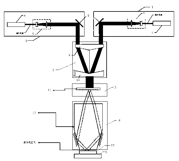
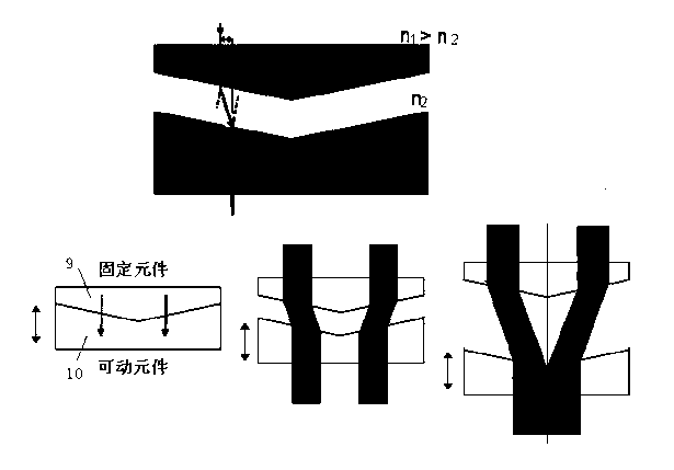
[0034] Embodiment 1 of the present invention such as figure 1 As shown, the multi-light source interference exposure device includes two illumination units 1 , a light combining unit 2 , a diffraction unit 3 , an interference unit 4 and a stage 5 and five major parts. The lighting unit 1 includes a light source 6 , a beam expander 7 and a reflector 8 , which converts the light emitted by two sets of laser light sources into parallel light spots, and enters the light combining unit 2 through two sets of reflectors 8 . The light combining unit 2 is composed of two wedge prisms 9 and 10 . The diffraction unit 3 is a phase grating 11 , the interference unit 4 is a converging prism 12 , and the stage 5 unit includes a wafer stage and a silicon wafer 13 .

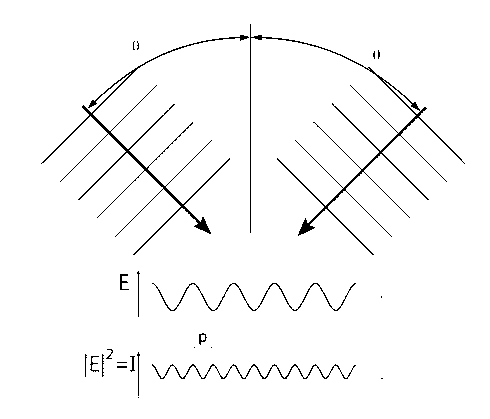
[0035] The working process of the device is as follows: by 2 light sources 6, usually lasers, each sends a beam of coherent beams (in the present invention, interference will not occur between 2 beams of coherent beams sent by 2...

Embodiment 2

[0046] The second embodiment of the present invention is as Figure 6 As shown, it also includes five parts: an illumination unit 1 , an optical unit 2 , a diffraction unit 3 , an interference unit 4 and a stage 5 .

[0047] In this embodiment, the light-merging unit and the light-merging principle are the same as those in Embodiment 1.

[0048] It differs from Example 1 in the use of different interference elements. The interfering element in the present embodiment is a rhombic prism 14, and its light path diagram is as follows Figure 7 As shown, therefore the interference exposure forms the fringe period (pitch):

[0049] (4)

[0050] And +1, -1 order diffraction angle θ is:

[0051] (5)

[0052] Here Pitch1 is the period of the diffraction grating. Assuming that the direction of the diffracted light in the prism is parallel to the optical axis, the wedge angle of the prism It is defined by the following formu...

Embodiment 3

[0059] The third embodiment of the present invention is as Figure 8 As shown, it includes four parts: an illumination unit 1 , a light combining unit 2 , an interference unit 4 and a stage 5 .

[0060] In this embodiment, the light-merging unit and the light-merging principle are the same as those in Embodiment 1.

[0061] It differs from Embodiment 1 in that there is no diffraction unit, and the interference elements are also different. The interfering element in the present embodiment is a trapezoidal prism 15, and its light path figure is as follows Figure 9 shown. The key point of splicing and interference here is that half of the spot of each beam of parallel light is incident on one surface of the trapezoidal prism 15, and the other half is incident on the surface at another angle, so that two parts of the beam emitted by the same laser interfere through the trapezoidal prism 15, The interference light produced by each of the two beams of light is then focused on th...


PUM


Abstract

The invention discloses a multi-light-source interference exposure device. The multi-light-source interference exposure device comprises an illumination unit, a light combining unit and an interference unit along a light propagation direction in sequence, wherein the illumination unit comprises multiple laser light sources which respectively generate a coherent light beam, the light combining unit splices the multiple coherent light beams sent by multiple laser light sources, and the interference unit sends multiple coherent beams spliced by the light combining unit outwards to a focal plane of the interference exposure device to respectively carry out interference imaging. The multi-light-source interference exposure device is simple in structure, high in resolution ratio, continuously adjustable in exposure pattern period, and adjustable in size of an exposure field, and improves producing efficiency.

Description

technical field [0001] The invention relates to the technical field of photolithography, in particular to a multi-light source interference exposure device used in photolithography devices. Background technique [0002] Under the current background that the line width CD in the field of semiconductor manufacturing technology generally enters below 90nm, using the method of optical projection exposure, in order to produce high-resolution periodic patterns within a certain exposure field range, a high-resolution mask is required. It is equipped with a large numerical aperture NA objective lens, resulting in a smaller depth of focus. As the size of the substrate becomes larger (such as 12-inch silicon wafer, sapphire substrate, etc.), it is often difficult to obtain a good substrate flatness, so it is necessary to introduce a complex, high-precision focusing and leveling system to ensure that the exposure surface of the substrate is in the within the depth of focus of the proj...

Claims


Application Information

Patent Timeline
Patent Type & Authority Applications(China)
IPC IPC(8): G03F7/20G02B27/10G02B27/44
Inventor 闻人青青
Owner SHANGHAI MICRO ELECTRONICS EQUIP (GRP) CO LTD
Learn More