
Display substrate, display panel and display device

A display substrate and display panel technology, which is applied in nonlinear optics, instruments, optics, etc., can solve the problems of affecting the reflectivity of reflective display panels, affecting the aperture ratio of reflective display panels, and cross-color display screens, so as to avoid cross-color Color phenomenon, reduce area requirement, increase aperture ratio and reflectivity effect

Inactive Publication Date: 2017-03-08
BOE TECH GRP CO LTD
View PDF9 Cites 7 Cited by
  • Summary
  • Abstract
  • Description
  • Claims
  • Application Information

AI Technical Summary

Problems solved by technology

The array substrate is provided with a reflective pattern to reflect the incident light of the display panel into the outgoing light for displaying the picture; the opposite substrate is provided with a color filter layer. Generally, the color filter layer includes three types: red, green and blue. Color filters, in order to prevent the side light from passing through the adjacent filter of another color from the filter of one color to cause cross-color phenomenon in the display screen, the solutions of the prior art are in different A black matrix is ​​set between the color filters of the color for light shielding, and the black matrix is ​​a non-transmitting pattern, so it will more or less affect the aperture ratio of the reflective display panel, thereby affecting the reflectivity of the reflective display panel

Method used


Image

  • Display substrate, display panel and display device
  • Display substrate, display panel and display device
  • Display substrate, display panel and display device

Examples


Embodiment Construction

[0025] In order to make the technical problems, technical solutions and advantages to be solved by the present invention clearer, the following will describe in detail with reference to the drawings and specific embodiments.

[0026] The present invention provides a solution to the problem of relatively low reflectivity of the existing reflective display panel.

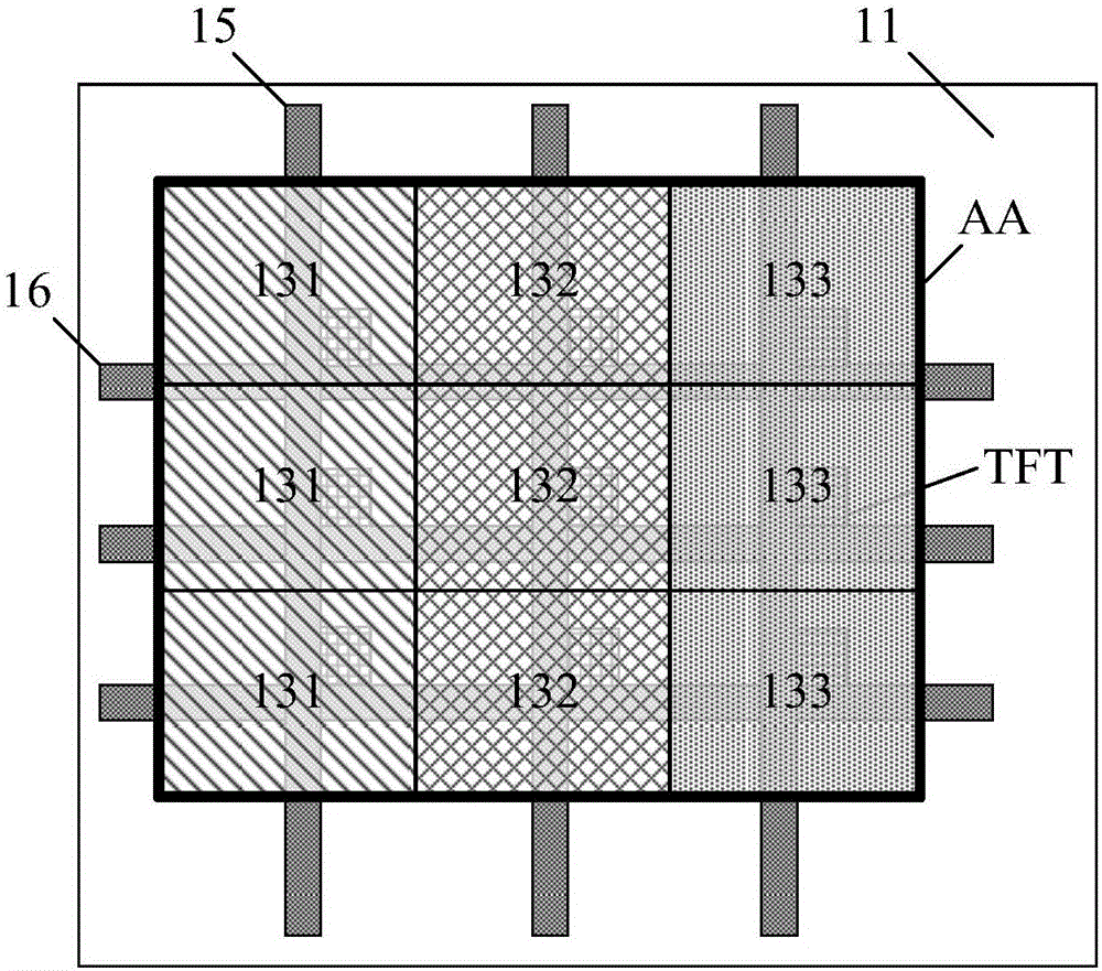
[0027] On the one hand, embodiments of the present invention provide a display substrate, such as figure 1 shown, including:

[0028] Substrate substrate 11;

[0029] Thin film transistor TFT arrays, gate lines ( figure 1 Not shown, the gate line is connected to the gate electrode G of the thin film transistor), the data line ( figure 1 Not shown, the data line is connected to the source electrode S of the thin film transistor);

[0030] The reflective pattern 12 positioned on the gate line, the data line and the thin film transistor TFT array is used to reflect the incident light to form the outgoing light of the...


PUM


Abstract

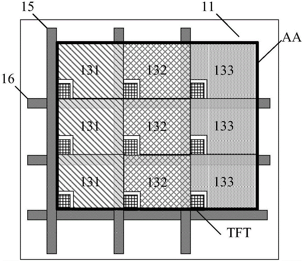
The invention provides a display substrate, a display panel and a display device. The display substrate comprises a substrate base plate, a grid line, a data line, a film transistor array, a reflection pattern and a color filter layer, wherein the grid line, the data line and the film transistor array are located on the substrate base plate; the reflection pattern is located on the grid line, the data line and the film transistor array and used for reflecting incident rays so as to form emergent rays for forming a display frame; and the color filter layer is located on the reflection pattern. According to the scheme provided by the invention, the color filter layer (namely, the pattern of a color filter) is arranged on the substrate base plate for reflecting the pattern, so that the color filter layer is closer to the reflection pattern, the horizontal transmission paths of the reflected rays passing by the color filter layer can be reduced and the cross color phenomenon can be further avoided. Obviously, on the basis of the scheme provided by the invention, the function of a black matrix can be reduced, i.e., the area of the black matrix to be arranged is greatly reduced and the opening rate and reflectivity of the display base plate can be further increased.

Description

technical field [0001] The present invention relates to the field of display technology, in particular to a display substrate, a display panel and a display device. Background technique [0002] As consumers have higher and higher requirements for display products, panel manufacturers have begun to make efforts in the development direction of display products with high transmittance, low power consumption, and thinner and lighter. At present, reflective display is a good technology to solve low power consumption. However, the current reflective display panel has relatively low reflectivity, so the brightness of the display screen is insufficient, which affects the viewing effect. [0003] Among them, the aperture ratio of the reflective display panel is an important index reflecting the reflectivity. The existing reflective display panel mainly includes an array substrate and an opposite substrate for forming a panel structure with the array substrate. The array substrate ...

Claims


Application Information

Patent Timeline
Patent Type & Authority Applications(China)
IPC IPC(8): G02F1/1335G02F1/1362
CPCG02F1/133514G02F1/1362G02F1/136222
Inventor 王英涛姚继开
Owner BOE TECH GRP CO LTD
Learn More