
Simulation Model and Simulation Method of Junction Field Effect Transistor

A technology of field effect transistors and simulation models, which is applied in special data processing applications, instruments, calculations, etc., and can solve problems that cannot meet the requirements of simulation accuracy

Active Publication Date: 2019-08-20
CSMC TECH FAB2 CO LTD
View PDF4 Cites 0 Cited by
  • Summary
  • Abstract
  • Description
  • Claims
  • Application Information

AI Technical Summary

Problems solved by technology

[0002] Junction Field-Effect Transistor (JFET) is widely used in the design of various analog circuits, and the accuracy requirements of device simulation models in circuit design are also getting higher and higher. The simulation software of Synopsys and Cadence The provided JFET model can no longer meet the simulation accuracy requirements

Method used


Image

  • Simulation Model and Simulation Method of Junction Field Effect Transistor
  • Simulation Model and Simulation Method of Junction Field Effect Transistor
  • Simulation Model and Simulation Method of Junction Field Effect Transistor

Examples


Embodiment Construction

[0071] Further description will be given below in conjunction with the accompanying drawings and embodiments.

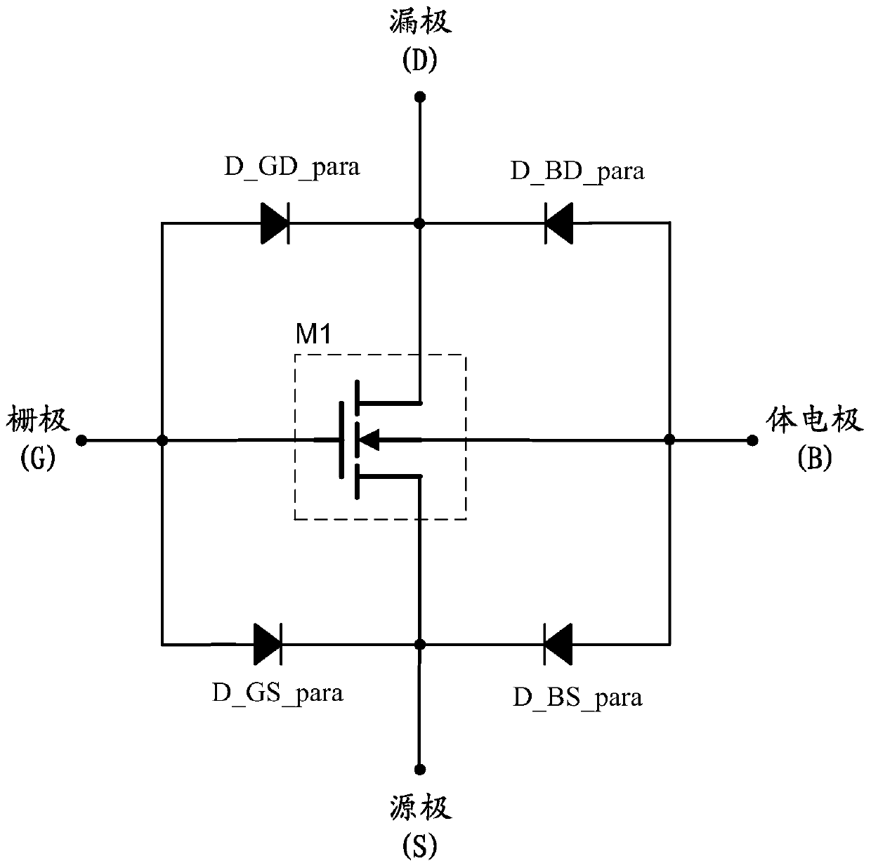
[0072] figure 1 It is the equivalent circuit structure of the simulation model of the junction field effect transistor of an embodiment. The simulation model of the junction field effect transistor includes a core field effect transistor model M1, a first diode model D_GD_para, a second diode model D_GS_para, a third diode model D_BD_para, and a fourth diode model D_BS_para.

[0073]The current and voltage characteristics of the core field effect transistor model M1 are fitted using the parameters of BSIM3 / BSIM4. BSIM3 / BSIM4 is a circuit simulation standard developed by the University of California, Berkeley. Starting from the third generation of BSIM3, the simulation standard is based on the physical model, based on quasi-two-dimensional analysis, and solves the physical characteristics of the device when it is working. In order to improve the accuracy in specifi...


PUM


Abstract

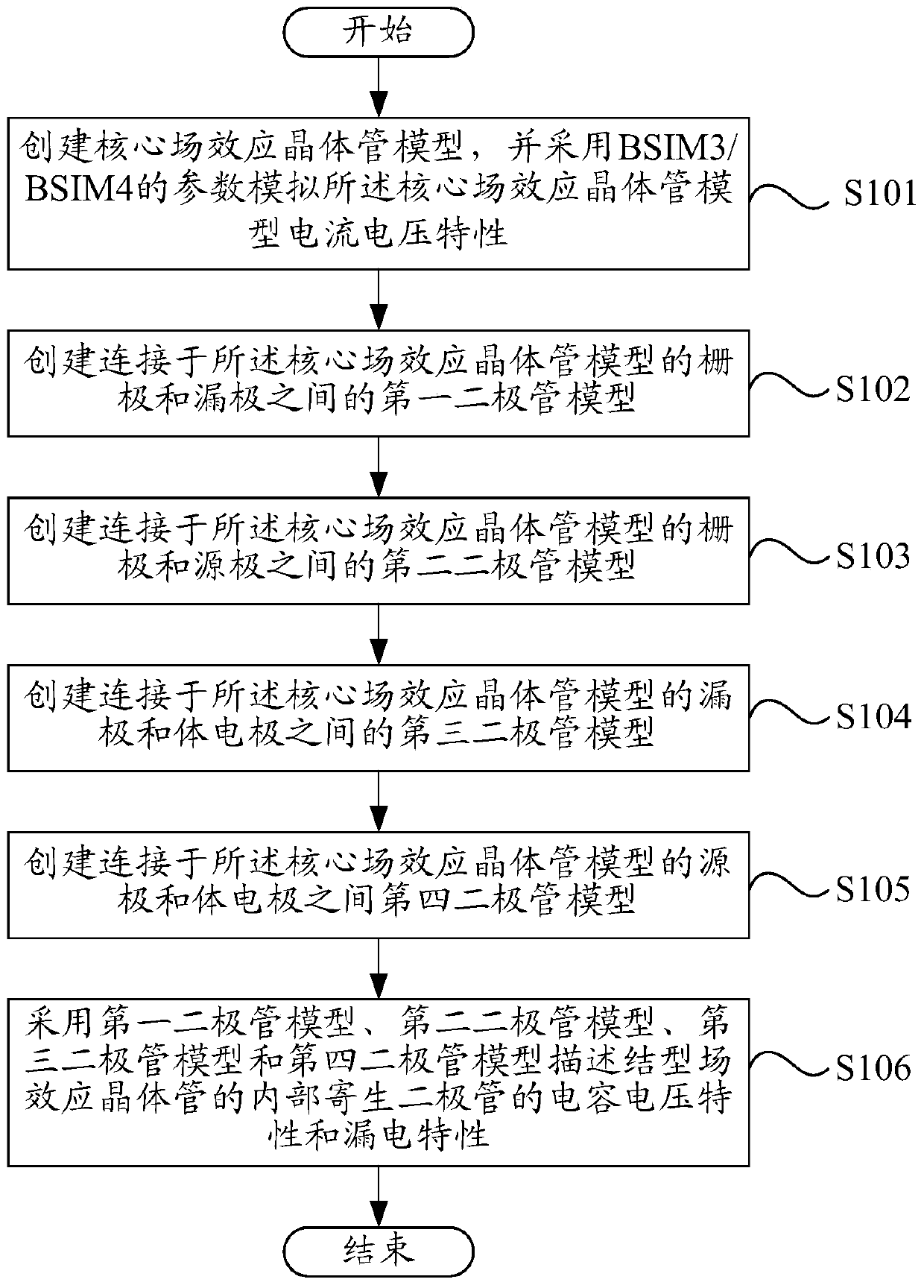
The invention relates to a simulation model of a junction field-effect transistor. The simulation model comprises a core field-effect transistor model, a first diode model, a second diode model, a third diode model and a fourth diode model, wherein a current-voltage characteristic of the core field-effect transistor model is fit by adopting parameters of BSIM3 / BSIM4; the first diode model is connected between a grid and a drain of the core field-effect transistor model; the second diode model is connected between the grid and a source of the core field-effect transistor model; the third diode model is connected between the drain of the core field-effect transistor model and a body electrode; the fourth diode model is connected between the source of the core field-effect transistor model and the body electrode; and the first diode model, the second diode model, the third diode model and the fourth diode model are used for describing a capacitance-voltage characteristic and a leakage current characteristic of an internal parasitic diode of the junction field-effect transistor. Furthermore, the invention further relates to a simulation method of the junction field-effect transistor. The simulation precision of the junction field-effect transistor is higher.

Description

technical field [0001] The invention relates to the technical field of device simulation, in particular to a simulation model of a junction field effect transistor and an application method thereof. Background technique [0002] Junction Field-Effect Transistor (JFET) is widely used in the design of various analog circuits, and the accuracy requirements of device simulation models in circuit design are also getting higher and higher. The simulation software of Synopsys and Cadence The provided JFET model can no longer meet the simulation accuracy requirements. Contents of the invention [0003] Based on this, it is necessary to provide a simulation model of a JFET with high simulation accuracy. [0004] A simulation model of a junction field effect transistor, including: [0005] The core field effect transistor model, whose current and voltage characteristics are fitted with the parameters of BSIM3 / BSIM4; [0006] A first diode model, connected between the gate and the...

Claims


Application Information

Patent Timeline
Patent Type & Authority Patents(China)
IPC IPC(8): G06F17/50
Inventor 刘新新
Owner CSMC TECH FAB2 CO LTD
Learn More