
Display device and method for preparing organic light emitting diode display panel

A technology of light-emitting diodes and display panels, applied in semiconductor/solid-state device manufacturing, electric solid-state devices, semiconductor devices, etc., can solve the problem of performance degradation of display devices, insufficient distribution of conductive particles 131, and reduced contact performance between pads 12 and FPC film 14 And other problems, to avoid short circuit, improve the effect of contact performance

Active Publication Date: 2017-03-08
EVERDISPLAY OPTRONICS (SHANGHAI) CO LTD
View PDF3 Cites 2 Cited by
  • Summary
  • Abstract
  • Description
  • Claims
  • Application Information

AI Technical Summary

Problems solved by technology

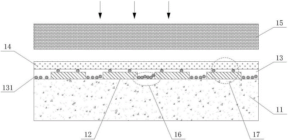
[0004] When adopting hot press head 15 to carry out hot pressing process to FPC film 14, promptly along figure 1 The above-mentioned FPC film 14 is pressed on the ACF film 13 in the direction indicated by the middle arrow. Due to the effect of pressure, the conductive particles 131 in the ACF film 13 will all converge on the panel 11 between the welding pads 12, so that The conductive particles 131 are gathered in the above-mentioned groove structure, and when too many conductive particles 131 are gathered, as in figure 1 In the region 16 shown in , it will lead to the generation of defects such as short-circuiting (Short) between adjacent pads 12 through the accumulated conductive particles 131; Convergence in the groove will lead to insufficient distribution of conductive particles 131 on the pad 12 (such as figure 1 Shown in the area 17), will reduce the contact performance between the welding pad 12 and the FPC film 14, and then cause the reduction of the performance of the display device prepared

Method used


Image

  • Display device and method for preparing organic light emitting diode display panel
  • Display device and method for preparing organic light emitting diode display panel
  • Display device and method for preparing organic light emitting diode display panel

Examples


Embodiment 1

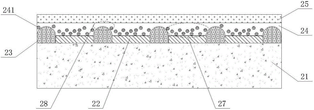
[0044] figure 2 It is a schematic diagram of the FOG structure in the embodiment of the present application; as figure 2 As shown, a display device in the embodiment of the present application may include, for example, a FOG structure formed after a hot-pressing process, and the above-mentioned display device may include:

[0045] A display panel 21, the display panel 21 may be an AMOLED glass substrate provided with a display module, or may be a panel for preparing other display devices, that is, the display panel 21 is provided with a light-emitting device; in addition , in order to facilitate the following explanation, define the surface of the display panel 21 through which the above-mentioned light-emitting device emits light is defined as the front surface (that is, the surface of the display substrate 21 located above in the figure of this embodiment is referred to as the front surface, and correspondingly, the surface located below is referred to as the front surface...

Embodiment 2

[0053] Figure 3-10 It is a schematic structural flow diagram of the method for preparing an organic light-emitting diode display panel in the embodiment of the present application; Figure 3-10 As shown, the present application also provides an organic light emitting diode display panel, which can be used to prepare a display device such as that in Embodiment 1 based on the traditional FOG structure (such as AMOLED FOG structure) preparation process, so as to effectively avoid adjacent The defects such as short circuit caused by the aggregation of conductive particles between the pads, and further improve the contact performance of the FOG structure in the display device, the above-mentioned methods specifically include:

[0054] First, if image 3 As shown, a display panel 31 is provided with a bonding area on its surface, and several welding pads 32 are provided on the surface of the display panel 31 located in the bonding area. The display panel 31 can be prepared with e...


PUM


Abstract

The invention relates to the technical field of semiconductor display, and particularly relates to a display device and a method for preparing an organic light emitting diode display panel. Convex blocks, which are higher than the upper surfaces of bonding pads, are arranged between the bonding pads on the display panel, so that conductive particles in an ACF film in a subsequent hot-pressing technological process are converged to an ACF film positioned above the bonding pads; therefore, the shortcomings of short-circuit between adjacent bonding pads caused by conductive particle convergence, and the like can be effectively avoided; and meanwhile, the contact performance between the display panel and an FPC film is effectively improved.

Description

technical field [0001] The invention relates to the technical field of semiconductor display, in particular to a display device and a method for preparing an organic light emitting diode display panel. Background technique [0002] At present, when setting FOG (Film on Glass, glass film) on the AMOLED display panel, since there are several welding pads ( Bonding Pad), and the several welding pads are all protruding from (that is, higher than) the surface of the panel, so in the process of hot pressing in the above-mentioned area, it is very easy to make the anisotropic conductive layer pressed on the panel and the welding pad The conductive particles in the anisotropic conductive film (ACF for short) are gathered between adjacent pads, thereby causing defects such as shorts between adjacent pads. [0003] figure 1 is a schematic cross-sectional view of the preparation of a traditional FOG structure; figure 1 As shown, an ACF film 13 is covered on the panel 11 provided wit...

Claims


Application Information

Patent Timeline
IPC IPC(8): H01L27/32H01L51/56
Inventor 施凯挺王俊闵
Owner EVERDISPLAY OPTRONICS (SHANGHAI) CO LTD
Learn More