Touch substrate, preparation method thereof and touch screen

A substrate and touch technology, applied in optics, instruments, electrical digital data processing, etc., can solve the problems of difficulty in meeting the requirements of the overall light transmittance of the functional hole area and the reduction of the overall light transmittance of the functional hole area.

Active Publication Date: 2017-03-15
BOE TECH GRP CO LTD +1
View PDF11 Cites 3 Cited by
  • Summary
  • Abstract
  • Description
  • Claims
  • Application Information

AI Technical Summary

Problems solved by technology

Although the etching of the disappearing layer in the functional hole area will make the overall chromaticity of the functional hole area meet the requirements, it is found in production that when etching the disappearing layer in the functional hole area, it is limited by the process. , there will always be vanishing material in the functional hole area, affected by these remaining residual vanishing materials, the overall light transmittance of the functional hole area will be reduced, and the overall light transmittance of the functional hole area is 87% to 90% %, it is difficult to meet the manufacturer's requirements for the overall light transmittance of the functional hole area

Method used


Image

  • Touch substrate, preparation method thereof and touch screen
  • Touch substrate, preparation method thereof and touch screen
  • Touch substrate, preparation method thereof and touch screen

Examples


Embodiment 1

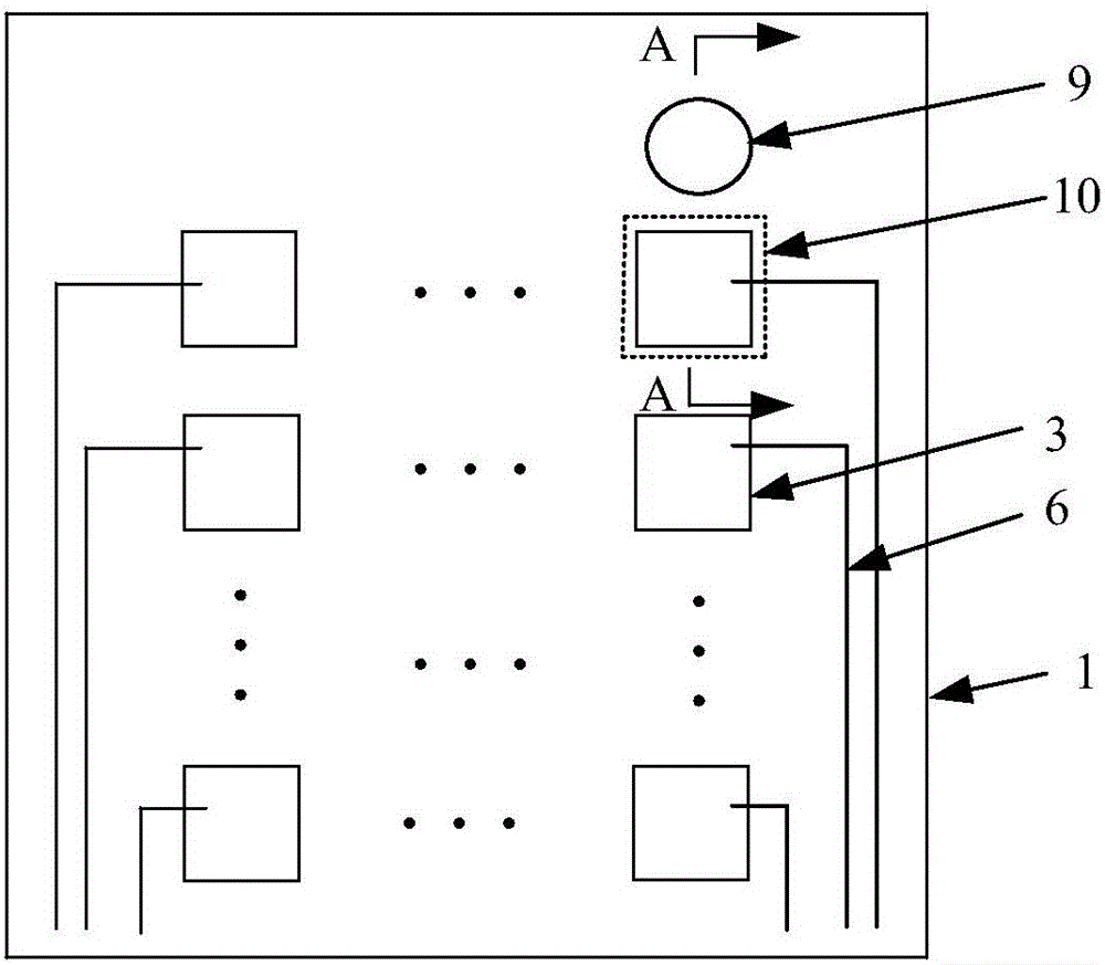
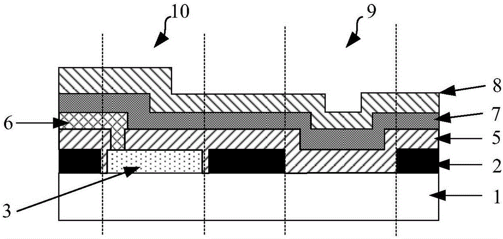
[0063] Figure 4 It is a schematic structural diagram of the touch substrate provided in Embodiment 1 of the present invention, Figure 5 The top view of the functional hole area in the touch substrate provided by the present invention, such as Figure 4 with Figure 5 As shown, the touch control substrate includes: a base substrate 1 on which a light-shielding pattern 2 is formed, and the light-shielding pattern 2 defines a touch area 10 and a functional hole area 9 . It should be noted that the situation of a touch area 10 and a function hole area 9 shown in the drawings is only for illustrative purposes, which will not limit the technical solution of the present invention, and those skilled in the art should know Yes, the shape, quantity, size, and position of the touch area 10 and the functional hole area 9 can be adjusted accordingly according to actual needs, and specific examples will not be illustrated here.

[0064] In the touch area 10 , a touch unit located above...

Embodiment 2

[0077] Image 6 A schematic structural diagram of the touch substrate provided in Embodiment 2 of the present invention, as shown in Image 6 as shown, Image 6 The touch substrate shown with the Figure 4 The difference of the touch substrate shown is that, the second insulating layer pattern 8 is arranged above the first disappearing pattern 71, and the anti-reflection pattern 4 is located above the second disappearing pattern 72 and is arranged on the same layer as the second insulating layer pattern 8. .

[0078] It should be noted that the material of the second insulating layer pattern 8 is generally an organic material, so when forming the second insulating layer pattern 8 and the anti-reflection pattern 4, it is only necessary to use a mask (Mask) to expose and develop the organic material to complete the composition. In addition, the film thickness (odd multiples of 1 / 4 light wave wavelength) of the material layer used to form the second insulating layer pattern 8...

Embodiment 3

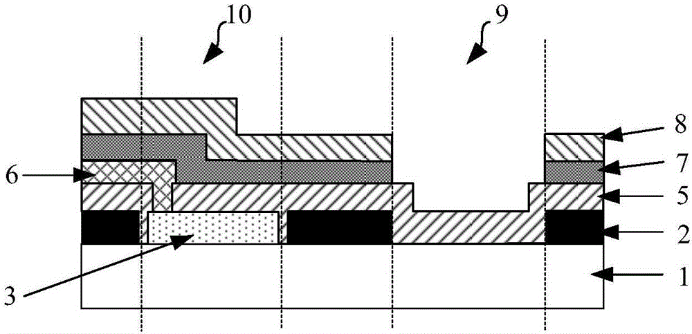
[0081] Figure 7 It is a flow chart of a method for manufacturing a touch substrate provided in Embodiment 3 of the present invention, Figure 8 for adoption Figure 7 Schematic diagram of the intermediate structure of the touch substrate prepared by the preparation method shown, as shown in Figure 7 with Figure 8As shown, the preparation method is used to prepare the touch substrate in the first embodiment above, and the preparation method includes:

[0082] Step S101 , forming a light-shielding pattern above the base substrate, where the light-shielding pattern defines a touch area and a functional hole area.

[0083] In step S101 , first deposit a layer of light-shielding material film on the base substrate 1 , and then pattern the light-shielding layer material to obtain a light-shielding pattern 2 , which defines the touch area 10 and the functional hole area 9 . Only one touch area 10 and one function hole area 9 are shown in the figure as an example.

[0084] Ste...


PUM


Abstract

The invention discloses a touch substrate, a preparation method thereof and a touch screen. The touch substrate comprises a substrate and a shading graph. In a touch area, a touch unit located above the substrate and a first blanking graph located above the touch unit are formed; and in a function hole area, a first insulating layer located above the substrate, a second blanking graph located above the first insulating layer and covering part of area in the function hole area and a permeability-increasing graph located above or below the second blanking graph and arranged corresponding to the second blanking graph are formed. According to the technical scheme, by setting the blanking graphs and the permeability-increasing graph in part of area in the function hole area, the area in the function hole area, which is provided with the blanking graphs and the permeability-increasing graph, has relatively high transmittance and chromaticity, the area which is not provided with the blanking graphs and the permeability-increasing graph has relatively low transmittance and chromaticity, so that at the time the overall high transmittance of the function hole area is relatively high, and the overall chromaticity is relatively low.

Description

technical field [0001] The invention relates to the field of display technology, in particular to a touch substrate, a preparation method thereof, and a touch screen. Background technique [0002] The 21st century is an era of rapid development, and the development of electronic products is also changing with each passing day. More and more touch elements are added to various electronic products, such as mobile phones, Pads, Notebooks, etc. have begun to use touch screens. At present, touch products on the market are designed with various functional holes (such as camera holes) in appearance. Adding functional holes can increase the added value of products and optimize customer experience. [0003] figure 1 is a top view of a touch substrate in the prior art, figure 2 for figure 1 The cross-sectional view in the A-A direction, such as figure 1 with figure 2 As shown, in order to realize the touch function, it is necessary to sequentially form a light-shielding pattern...

Claims


Application Information

Patent Timeline
IPC IPC(8): G06F3/041G06F3/044G02F1/1333G02F1/1335
CPCG02F1/13338G02F1/133512G06F3/041G06F3/044G06F3/0412G06F2203/04103
Inventor 王静谢晓冬何敏张贵玉许邹明郑启涛田新斌李冬
Owner BOE TECH GRP CO LTD
Why Eureka
Try Eureka