Method for producing electroplated copper layer with preferential orientation growth structure, and application thereof

A technology of preferential orientation and electroplating copper layer, which is applied to electrodes, circuits, electrical components, etc., can solve problems such as poor thermal stability, easy chip failure, and reliability problems, and achieve a wide range of current densities, ensuring service reliability, The effect of ensuring reliability

Active Publication Date: 2017-03-22
SUZHOU SHINHAO MATERIALS
View PDF16 Cites 5 Cited by
  • Summary
  • Abstract
  • Description
  • Claims
  • Application Information

AI Technical Summary

Problems solved by technology

[0003] With the continuous improvement of wafer-level packaging density, the size of Cu pillars and RDL Lines is getting smaller and smaller. The bonding fastness of Cu pillars and RDLLines to the wafer substrate determines the service reliability of the chip. After the subsequent removal of the copper seed layer In the process, the structure of the existing electroplated copper layer determines that Under Cut defects will inevitably appear. When the size of Cu pillars and RDL Lines becomes smaller and smaller, the existence of Under Cut makes the chip extremely easy to fail during use, reliable sexual problems
[0004] The electroplated copper layer is in direct contact with the sputtered copper seed layer. When the internal structure of the electroplated copper layer is disordered and irregular, the bonding fastness to the copper seed layer is poor and the thermal stability is poor. Poor, follow-up reliability problems

Method used


Image

  • Method for producing electroplated copper layer with preferential orientation growth structure, and application thereof
  • Method for producing electroplated copper layer with preferential orientation growth structure, and application thereof
  • Method for producing electroplated copper layer with preferential orientation growth structure, and application thereof

Examples


Embodiment 1

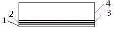
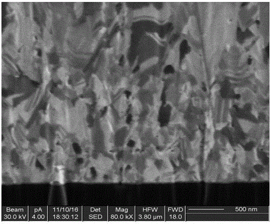
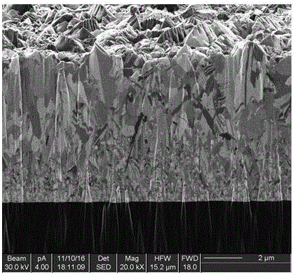
[0032] see figure 1 As shown, a copper layer with a preferential orientation growth structure in the Z-axis direction includes a wafer substrate 1, an adhesion layer 2, a copper seed layer 3 and an electroplated copper layer 4 in sequence, and the electroplated copper layer 4 contains a Z-axis The approximate columnar crystal structure grown in the preferred orientation in the Z-axis direction has a large grain size and few grain boundaries in the Z-axis direction, and the small grain size and many grain boundaries in the X-axis direction .

[0033] Preferably, the wafer substrate 1 is silicon or silicon germanium semiconductor material, or a chip or device containing silicon or silicon germanium, and the adhesion layer 2 is a titanium layer.

[0034] Preferably, the copper seed layer 3 is prepared by magnetron sputtering, and the copper seed layer 3 is connected to the electroplated copper layer 4 .

Embodiment 2

[0036] A method for preparing an electroplated copper layer with a preferred orientation growth structure, using a direct current electroplating process, the composition of the electroplating solution is copper sulfate 120-200g / L, sulfuric acid 50-150g / L, wetting agent 100-1000ppm, bright 5-50ppm agent, 40-100ppm non-dye-based leveling agent, and the rest is water;

[0037] The electroplating anode plate adopts phosphor copper plate, and the P element content in the phosphor copper plate is 0.03~150wt.%.

[0038] The current density is 1~18A / dm 2 ;

[0039] During the electroplating process, mechanical stirring is used to ensure uniform concentration in the plating solution and increase mass transfer.

[0040] Preferably, the wetting agent is polyethylene glycol or polyethyleneimine, the brightener is sodium polydithiodipropane sulfonate, and the non-dye-based leveling agent is a nitrogen-containing organic heterocyclic compound.

[0041] The electroplated copper layer with...


PUM

PropertyMeasurementUnit
hardnessaaaaaaaaaa

Abstract

The invention discloses a method for producing an electroplated copper layer with a preferential orientation growth structure, and belongs to the field of semiconductor wafer packaging. The copper layer with a preferential orientation growth structure comprises a wafer substrate, an adhesive layer, a copper seed crystal layer and an electroplated copper layer, and the electroplated copper layer has a Z-axial preferential orientation growth structure. The Z-axial preferential orientation growth structure is produced on the wafer substrate by adopting a non-dye leveling agent through a traditional direct-current electroplating technology, and the corrosion reaction rate, the hardness and the tensile strength of the electroplated copper layer in an X-axial direction and a Z-axial direction are different.

Description

technical field [0001] The invention belongs to the field of electroplating, and in particular relates to a method for preparing an electroplated copper layer. Background technique [0002] Copper metal is an excellent material for chip interconnection due to its advantages of good electrical conductivity, thermal conductivity, low melting point and good ductility. Copper electroplating is the method of choice for copper interconnects. Higher I / O count, higher packaging density, smaller package structure, more reliable performance and thermal stability are the major trends in advanced semiconductor packaging. Packaging forms such as wafer-level packaging chip-scale packaging (WLCSP), 3D stacked packaging (3D IC packaging), and POP (packaging on packaging) are all concrete manifestations of this trend. [0003] With the continuous improvement of wafer-level packaging density, the size of Cu pillars and RDL Lines is getting smaller and smaller. The bonding fastness of Cu pil...

Claims


Application Information

Patent Timeline
Patent Type & Authority Applications(China)
IPC IPC(8): C25D3/38C25D7/12
CPCC25D3/38C25D7/12C25D7/123C25D17/10C25D21/10H01L21/2885H01L23/53238H01L21/76873
Inventor 张芸朱自方马涛陈路明王靖
Owner SUZHOU SHINHAO MATERIALS
Why Eureka
Try Eureka