Display panel and display device
A technology for display panels and substrates, applied in optics, instruments, nonlinear optics, etc., can solve problems such as color filter substrates without liquid crystal display panels, and achieve the effects of improving display quality, reducing costs, and improving display color gamut
- Summary
- Abstract
- Description
- Claims
- Application Information
AI Technical Summary
Problems solved by technology
Method used
Image

Examples
Embodiment 1
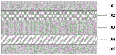
[0062] see Figure 9 , a display panel provided in an embodiment of the present application includes:
[0063] Blue backlight 106, lower substrate 105 on blue backlight 106, TFT array 104 on lower substrate 105, PDLC layer 103 on TFT array 104, quantum dots on PDLC layer 103 Layer 102, the upper substrate 101 above the quantum dot layer 102.
[0064] Wherein, a PS107 is provided in the PDLC layer 103;
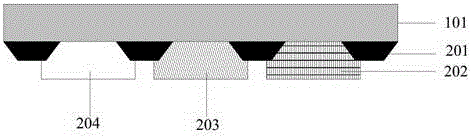
[0065] The quantum dot layer 102 is provided with a black matrix 201 and a blank area 204 , a green quantum dot layer 301 , and a red quantum dot layer 303 . The green quantum dot layer 301 constitutes a green sub-pixel region, and the red quantum dot layer 303 constitutes a red pixel region.
[0066] Wherein, the quantum rod materials that can be used for the green quantum dot layer 301 and the red quantum dot layer 303 include: GaAS, GaP, InGaAs and the like.
[0067] The blue backlight 106 is not limited to a blue backlight, as long as the wavelength can excite quantum d...
Embodiment 2
[0076] On the basis of the first embodiment, further, a blue quantum dot layer or a transparent resin or a blue resin may be provided in the blank area 204 .
[0077] Due to the low light conversion efficiency of quantum dots, when exciting red quantum dots, there may be light leakage from the backlight, resulting in color mixing. In order to prevent light leakage, red, green, and blue color filter layers can be prepared respectively on top of the red, green, and blue quantum dot layers, so that the light from the backlight can be filtered through the color filter layers. Wherein, the color filter layer is the resin layer where the red resin layer, the green resin layer and the blue resin layer are located.
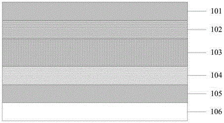
[0078] Therefore, see Figure 10 , a display panel provided in this embodiment includes:
[0079] Blue backlight 106, lower substrate 105 on blue backlight 106, TFT array 104 on lower substrate 105, PDLC layer 103 on TFT array 104, quantum dots on PDLC layer 103 Layer ...
Embodiment 3
[0083] see Figure 11 , the display panel provided in this embodiment includes:
[0084] Blue backlight 106, the lower substrate 105 on the blue backlight 106, the TFT array 104 on the lower substrate 105, the quantum dot layer 102 on the TFT array 104, the quantum dot layer 102 on the quantum dot layer 102 The PDLC layer 103 and the upper substrate 101 on the PDLC layer 103 .
[0085] Wherein, a PS 107 is provided in the PDLC layer 103;
[0086] The quantum dot layer 102 is provided with a black matrix 405 and a blank area 503 , a red quantum dot layer 402 , and a green quantum dot layer 404 . The green quantum dot layer 404 constitutes a green sub-pixel region, and the red quantum dot layer 402 constitutes a red pixel region. A green resin layer 403 is further disposed on the green quantum dot layer 404 , and a red resin layer 401 is further disposed on the red quantum dot layer 402 .
[0087] Embodiment 3 is the same as Embodiment 2. In order to prevent backlight from b...
PUM
| Property | Measurement | Unit |
|---|---|---|
| diameter | aaaaa | aaaaa |
Abstract
Description
Claims
Application Information
 - R&D
- Intellectual Property
- Life Sciences
- Materials
- Tech Scout
- Unparalleled Data Quality
- Higher Quality Content
- 60% Fewer Hallucinations
Browse by: Latest US Patents, China's latest patents, Technical Efficacy Thesaurus, Application Domain, Technology Topic, Popular Technical Reports.
© 2025 PatSnap. All rights reserved.Legal|Privacy policy|Modern Slavery Act Transparency Statement|Sitemap|About US| Contact US: help@patsnap.com