Germanium channel quantum well field effect transistor with low power consumption and high performance

A field-effect transistor, high-performance technology, applied in semiconductor devices, electrical components, circuits, etc., can solve the problems of low stability, affect transistor performance, affect device reliability, etc., achieve large operating current, and improve device operating current. Effect

Inactive Publication Date: 2017-03-29
ZHEJIANG UNIV
View PDF4 Cites 2 Cited by
  • Summary
  • Abstract
  • Description
  • Claims
  • Application Information

AI Technical Summary

Benefits of technology

This new type of transistors called Germanium Channel Quantum Well (GPC) has several benefits compared with older types like Metal Oxides Semi conductive MOSFETs: they have higher performance at lower power levels due to their ability to control electron or hole movement more accurately by reducing layer thicknesses while maintaining good crystal quality for better electrical properties. Additionally, these devices are able to work without any problems caused from charge carriers being scattered around them during operation.

Problems solved by technology

This patented technical solution discusses how improving the properties (performance) of electronic components made from different types of materials like gallium arsenic and gadolinia). Specifically, the challenge being addressed involves achieving stable contact between metal atoms without causing unwanted diffusion within the crystal lattice itself. Additionally, the goal sought after is developing novel materials called Gunnovacrosium carbon nitride (GNC), specifically including MoOx/MoS5/Si02 nanoparms, where Ge occupies most volume compared to Si. These materials provide improved electrical conductivity while maintaining excellent work function capabilities.

Method used


Image

  • Germanium channel quantum well field effect transistor with low power consumption and high performance
  • Germanium channel quantum well field effect transistor with low power consumption and high performance
  • Germanium channel quantum well field effect transistor with low power consumption and high performance

Examples


Embodiment Construction

[0020] In order to describe the present invention more specifically, the technical solution of the present invention and its related principles and manufacturing process will be described in detail below in conjunction with the accompanying drawings and specific embodiments.

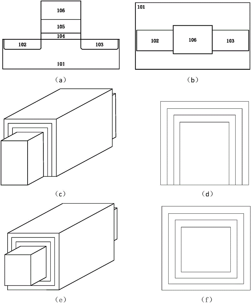
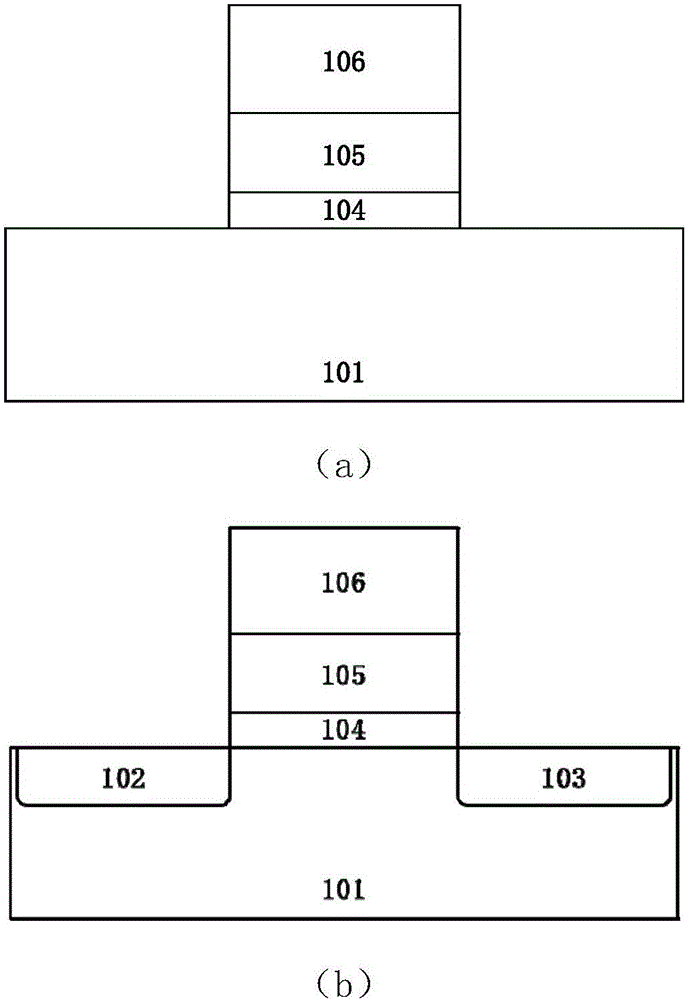
[0021] Such as figure 1 As shown, the present invention provides a quantum well field effect transistor with low power consumption and high performance germanium channel, including a semiconductor germanium substrate 101; the semiconductor germanium substrate 101 has a source implantation region 102 and a drain implantation region 103 The surface of the semiconductor germanium substrate 101 between the source injection region 102 and the drain injection region 103 covers the two-dimensional material passivation layer 104, the gate insulating layer 105 and the gate electrode 106 in sequence; the source injection region 102 and the drain The end injection regions 103 are all provided with N+ or P+ active i...


PUM


Abstract

The invention discloses a germanium channel quantum well field effect transistor with a low power consumption and a high performance. The germanium channel quantum well field effect transistor comprises a semiconductor germanium substrate; the semiconductor germanium substrate is provided with a source end injection region and a drain end injection region; a two-dimensional material passivation layer, a gate insulation layer and a grid electrode are covered on a surface of the semiconductor germanium substrate in sequence; and each of the source end injection region and the drain end injection region is provided with an N+ active injection region or a P+ active injection region. When the quantum well transistor having above structure is in work, a working current larger than the traditional germanium-based metal oxide semiconductor field effect transistor can be obtained; when the number of layers of a two-dimensional material in a grid laminated layer is reduced, an energy band structure is changed, so a relative position deviation between the energy band structure corresponding to the special number of the layers and the energy band structure of germanium enables a germanium channel to form a quantum well; and therefore, the transportation space for two carriers, namely electron and hole, can be effectively limited, the influence of carrier scattering on migration rate is reduced, the working current of a device is improved, and the P type and N type transistors with the low power consumption and the high performance are realized.

Description


Claims


Application Information

Patent Timeline
Owner ZHEJIANG UNIV
Why Eureka
Try Eureka