LDMOS transistor and formation method thereof

A technology of transistors and body regions, which is applied in the manufacture of transistors, semiconductor devices, semiconductor/solid-state devices, etc., can solve the problems of lateral double diffused field effect transistors (LDMOS transistors, etc., whose performance needs to be improved, and achieve improved channel doping uniformity, The effect of preventing short channel effect and preventing influence

Active Publication Date: 2018-01-09
SEMICON MFG INT (SHANGHAI) CORP +1
View PDF3 Cites 9 Cited by
  • Summary
  • Abstract
  • Description
  • Claims
  • Application Information

AI Technical Summary

Problems solved by technology

[0004] However, the performance of the existing lateral double diffused field effect transistor (LDMOS transistor) still needs to be improved.

Method used


Image

  • LDMOS transistor and formation method thereof
  • LDMOS transistor and formation method thereof
  • LDMOS transistor and formation method thereof

Examples


Embodiment Construction

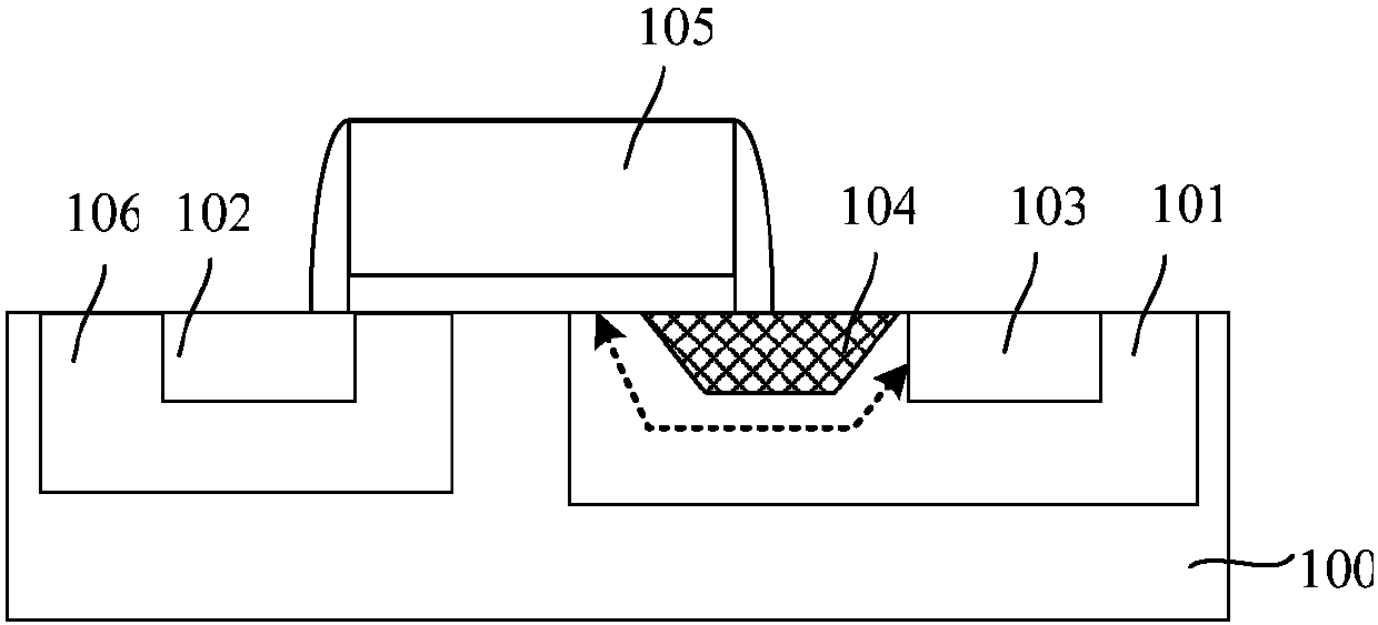
[0033] As mentioned in the background, the performance of the existing lateral double diffused field effect transistor (LDMOS transistor) still needs to be improved, for example, the operating current value of the existing LDMOS transistor still needs to be improved.

[0034] Research has found that the operating current of LDMOS transistors in the prior art is limited by the on-resistance between the source region and the drain region, and it is difficult to continue to increase, although it can be achieved by reducing the width (or size) of the channel between the source region and the drain region or increasing The doping dose of the source region and the drain region increases the operating current value, but correspondingly reduces the breakdown voltage of the LDMOS transistor and causes short channel effects or changes in other electrical properties.

[0035] Further studies have found that when the existing process forms the source region and the drain region through the i...


PUM


Abstract

A LDMOS transistor and a formation method thereof are provided; the method comprises the following steps: providing a semiconductor substrate, and forming a shallow trench isolation structure in the semiconductor substrate; forming a drift region in the semiconductor substrate, wherein the drift region encloses the shallow trench isolation structure; forming a body region in the semiconductor substrate on the drift region side; forming a gate structure crossing and covering partial the body region, the drift region and the shallow trench isolation structure; forming a drain region in the driftregion on the gate structure side; forming a source region in the body region on the other side of the gate structure; forming a first shallow doping region in the drain region on the gate structureside and in the drift region on the gate structure bottom, wherein the first shallow doping region doping type is same with the drain region doping type, and the first shallow doping region depth is smaller than the drain region depth and drift region depth. The method can improve the LDMOS transistor working current.

Description

technical field [0001] The invention relates to the field of semiconductor manufacturing, in particular to an LDMOS transistor and a forming method thereof. Background technique [0002] The power field effect transistor mainly includes two types: a vertical double-diffused field effect transistor (VDMOS, Vertical Double-Diffused MOSFET) and a lateral double-diffused field effect transistor (LDMOS, Lateral Double-Diffused MOSFET). Among them, compared with the vertical double diffused field effect transistor (VDMOS), the lateral double diffused field effect transistor (LDMOS) has many advantages, for example, the latter has better thermal stability and frequency stability, higher gain and durability stability, lower feedback capacitance and thermal resistance, as well as constant input impedance and simpler bias current circuitry. [0003] In the prior art, a conventional N-type lateral double-diffused field effect transistor (LDMOS transistor) structure is as follows figu...

Claims


Application Information

Patent Timeline
Patent Type & Authority Applications(China)
IPC IPC(8): H01L21/336H01L29/78H01L29/06
CPCH01L21/26506H01L29/66659H01L29/7835H01L29/0847H01L29/1045H01L21/26586H01L29/0653H01L21/26513H01L21/76224H01L29/086H01L29/0865H01L29/0878H01L29/0882H01L29/1095H01L29/167H01L29/66681H01L29/7816
Inventor 赵猛
Owner SEMICON MFG INT (SHANGHAI) CORP
Why Eureka
Try Eureka