Semiconductor integrated circuit device

a technology of integrated circuits and semiconductors, applied in semiconductor devices, digital storage, instruments, etc., can solve the problems of increased current consumption, inability to switch word lines between selected states in time, etc., and achieve the effects of reducing leakage current, large parasitic capacitance, and increasing operating curren

Active Publication Date: 2006-08-17
RENESAS ELECTRONICS CORP
View PDF3 Cites 9 Cited by
  • Summary
  • Abstract
  • Description
  • Claims
  • Application Information

AI Technical Summary

Benefits of technology

[0008] In the technique disclosed in Patent Document 1, such a control signal as mentioned above is provided, and the reduction of leakage current is accomplished by power supply control. For this reason, an operating current due to the amplitude of the control signal and the like is produced. Therefore, varying the above control signal from memory cycle to memory cycle in synchronization with a clock signal or the like not only increases operating currents due to the amplitude of the control signal and the like. Alternately changing the potential of the power supply line Vddp, which has a relatively large parasitic capacitance because a large number of word drivers are connected, to 0.5V and to 1.0V, as mentioned above, poses a problem of increased current consumption. In addition, it is not practical in terms of the time required to switch word lines between selected state and deselected state. For this reason, the technique disclosed in Patent Document 1 brings about the power consumption reducing effect only when standby state is established for a certain period or longer.

Problems solved by technology

Alternately changing the potential of the power supply line Vddp, which has a relatively large parasitic capacitance because a large number of word drivers are connected, to 0.5V and to 1.0V, as mentioned above, poses a problem of increased current consumption.
In addition, it is not practical in terms of the time required to switch word lines between selected state and deselected state.

Method used


Image

  • Semiconductor integrated circuit device
  • Semiconductor integrated circuit device
  • Semiconductor integrated circuit device

Examples


Embodiment Construction

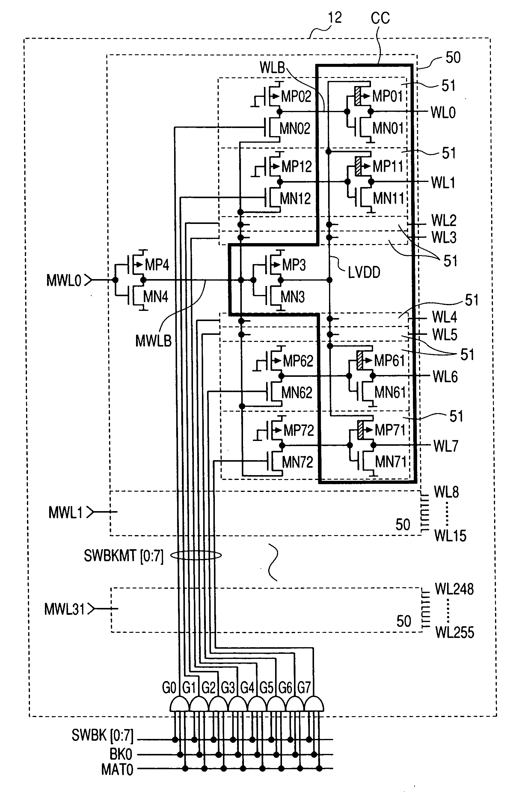
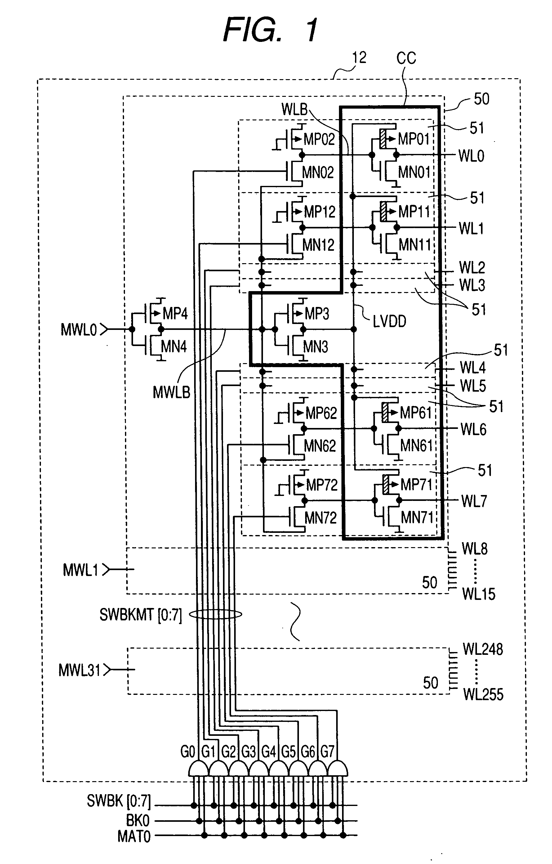
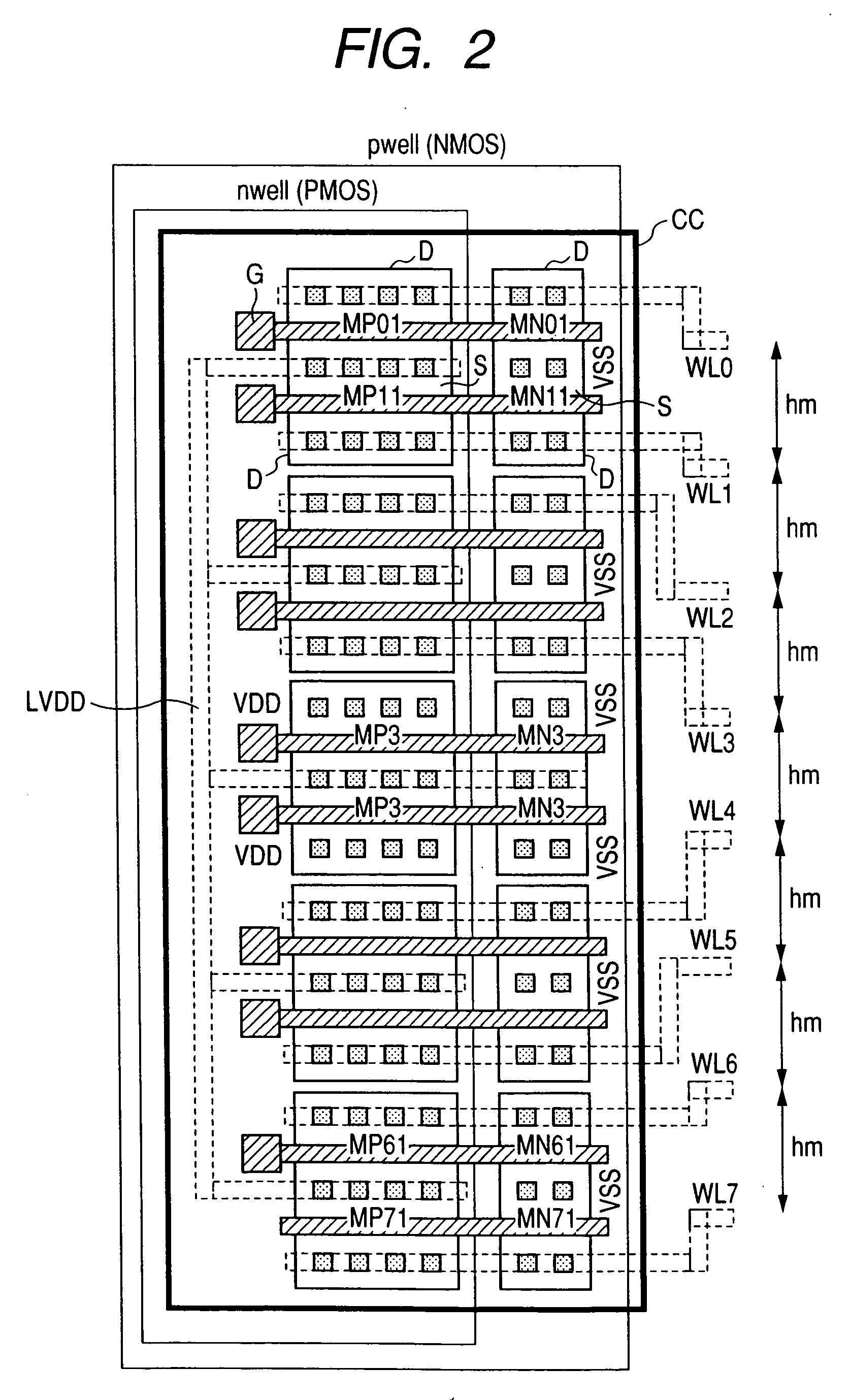
[0028]FIG. 4 is a block diagram of an embodiment of SRAM to which the present invention is applied. In the drawing, AX denotes X (row) address signal; AY denotes Y (column) address signal; Din denotes data input signal; CLK denotes clock signal; / R denotes read control signal; / W denotes write control signal; and DQ denotes data output signal. XAB denotes X address buffer, and YAB denotes Y address buffer. XDEC denotes X (row) decoder, which includes the predecoders and the word drivers described later. YDEC denotes Y (column) decoder, which includes the Y selection switch and the like described later. MARY denotes memory array, which is constructed by disposing static memory cells at the points at which the word lines and the bit lines intersect.

[0029] DIB denotes input buffer that takes in data input signals Din, and DOB denotes output buffer that sends out output signals. A write signal taken into the input buffer DIB is written into a selected memory cell in the memory array MA...


PUM


Abstract

A semiconductor integrated circuit device provided with a memory circuit having a word line selection circuit with reduced leakage current is provided. The memory circuit includes: second word lines with which memory cells are connected; multiple bit lines that are extended in a direction orthogonal thereto and electrically connected with memory cells corresponding to selected second word lines of a plurality of the second word lines; and word drivers, constructed of CMOS inverter circuits, that select or deselect the second word lines. The sources of p-channel MOSFETs that constitute a plurality of word drivers including second word lines corresponding to selected bit lines are supplied with a voltage at a level at which second word lines are selected. The sources of the p-channel MOSFETs of the other word drivers are supplied with a voltage corresponding to a level at which second word lines are deselected.

Description

CROSS-REFERENCE TO RELATED APPLICATION [0001] The present application claims priority from Japanese patent publication No. 2005-038650 filed on Feb. 16, 2005, the content of which is hereby incorporated by reference into this application. BACKGROUND OF THE INVENTION [0002] The present invention relates to a semiconductor integrated circuit device, and in particular to a technology effectively applicable to that provided with a memory circuit, such as a static RAM. [0003] As the power consumption of LSIs (Large Scale Integrated circuits) is reduced and the transistors (MOSFETs) in LSIs are microminiaturized, the power supply voltages of LSIs have been lowered. In a 0.13-μm process, for example, LSIs that operate on a power supply voltage of 1.2V are manufactured. In a case where the power supply voltage of LSI is lowered, the following measure is taken to prevent circuit performance (the operating speed of circuit) from being degraded: the threshold voltage (hereafter, abbreviated as...

Claims


Application Information

Patent Timeline
Patent Type & Authority Applications(United States)
IPC IPC(8): G11C8/00
CPCG11C8/08G11C8/14H01L27/04H10B10/00
Inventor SHINOZAKI, MASAOSHIMADU, DAISUKE
Owner RENESAS ELECTRONICS CORP
Why Eureka
Try Eureka