Carbon-nano-field emission cathode and manufacturing method and application

A field emission cathode and manufacturing method technology, applied in the field emission field, can solve the problems of poor stability and low emission current density, and achieve the effects of low interface resistance, improved emission stability, and excellent thermal conductivity

Active Publication Date: 2018-06-15
SHENZHEN INST OF ADVANCED TECH
View PDF6 Cites 10 Cited by
  • Summary
  • Abstract
  • Description
  • Claims
  • Application Information

AI Technical Summary

Problems solved by technology

[0004] The purpose of the present invention is to provide a carbon nanometer field emission cathode and its manufacturing method and application, aiming to solve the technical problems of low emission current density and poor stability of the carbon nanometer field emission cathode in the prior art

Method used


Image

  • Carbon-nano-field emission cathode and manufacturing method and application
  • Carbon-nano-field emission cathode and manufacturing method and application

Examples


Embodiment Construction

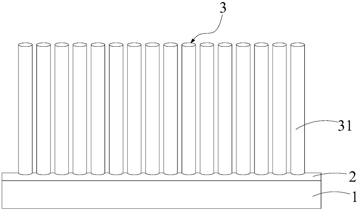
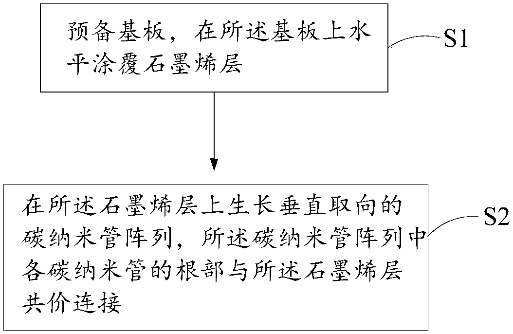
[0019] Embodiments of the present invention are described in detail below, examples of which are shown in the drawings, wherein the same or similar reference numerals designate the same or similar elements or elements having the same or similar functions throughout. The embodiments described below by referring to the figures are exemplary and are intended to explain the present invention and should not be construed as limiting the present invention.

[0020] In describing the present invention, it should be understood that the terms "length", "width", "upper", "lower", "front", "rear", "left", "right", "vertical", The orientation or positional relationship indicated by "horizontal", "top", "bottom", "inner", "outer", etc. are based on the orientation or positional relationship shown in the drawings, and are only for the convenience of describing the present invention and simplifying the description, rather than Nothing indicating or implying that a referenced device or element...


PUM


Abstract

The invention, which relates to the technical field of field emission, provides a carbon-nano-field emission cathode and a manufacturing method and application. The carbon-nano-field emission cathodecomprises a substrate, a graphene layer horizontally coated on the substrate, and a carbon nanotube array arranged on the graphene layer. Roots of all carbon nanotubes in the carbon nanotube array arein covalent linkage with the graphene layer. According to the invention, because the roots of all carbon nanotubes are in covalent linkage with the graphene layer, the interface resistance is extremely low and thus the carbon nanostructure has excellent conductivity, so that the opening electric field of the cathode is reduced obviously; the heat generated during the field emission process is lowand thus the cathode can be emitted stably at the high current, so that the operating current of the cathode is improved substantially. Moreover, because the three-dimensional covalent structure hasexcellent thermal conductivity, the emission stability of the cathode is improved.

Description

technical field [0001] The invention relates to the technical field of field emission, and in particular provides a carbon nanometer field emission cathode and a manufacturing method and application thereof. Background technique [0002] High-current vacuum electronic devices, including microwave tubes, X-ray tubes, electronic propulsion and charge control devices, are key components in the fields of communications, space technology, safety testing, and medical imaging. The cathode is the core component of high-current vacuum electronic devices, and metal hot cathodes are still used as the main electron emission source at present. Hot cathodes have defects such as large volume, large thermal radiation power consumption, long turn-on time, and material evaporation at high temperatures, which limit the development of vacuum electronic devices in the direction of miniaturization and integration. [0003] In recent years, nanomaterial field emission cold cathodes represented by...

Claims


Application Information

Patent Timeline
Patent Type & Authority Applications(China)
IPC IPC(8): H01J29/04H01J35/06H01J1/304H01J9/02
CPCH01J1/304H01J9/025H01J29/04H01J35/065H01J2201/30434H01J2201/30469H01J2209/0223H01J2235/062
Inventor 洪序达梁栋石伟
Owner SHENZHEN INST OF ADVANCED TECH
Why Eureka
Try Eureka