Field-effect transistor and preparation method thereof

A technology of field effect transistors and manufacturing methods, which is applied in semiconductor/solid-state device manufacturing, semiconductor devices, electrical components, etc., can solve the problems that reliability has not been well studied, and achieve fast switching speed, small leakage current, and shock The effect of high breakdown voltage

Inactive Publication Date: 2010-11-17
FUDAN UNIV
View PDF4 Cites 9 Cited by
  • Summary
  • Abstract
  • Description
  • Claims
  • Application Information

AI Technical Summary

Problems solved by technology

However, the source-drain field effect transistor purely composed of Schottky junctions also has many potential problems. Schottky junctions often have additional leakage current and soft breakdown. not well researched

Method used


Image

  • Field-effect transistor and preparation method thereof
  • Field-effect transistor and preparation method thereof
  • Field-effect transistor and preparation method thereof

Examples


Embodiment Construction

[0048]The structure and manufacturing process of the asymmetric source-drain field effect transistor proposed by the present invention will be described in detail below with reference to the accompanying drawings. In the following description, the same reference numerals denote the same components, and repeated description thereof will be omitted. In the following reference drawings, for convenience of description, the sizes of different layers and regions are enlarged or reduced, so the shown sizes do not necessarily represent actual sizes, nor do they reflect the proportional relationship of sizes.

[0049] It should be noted that many widely different embodiments may be constructed without departing from the spirit and scope of the present invention. It should be understood that the invention is not limited to the specific examples described in the specification, except as defined in the appended claims.

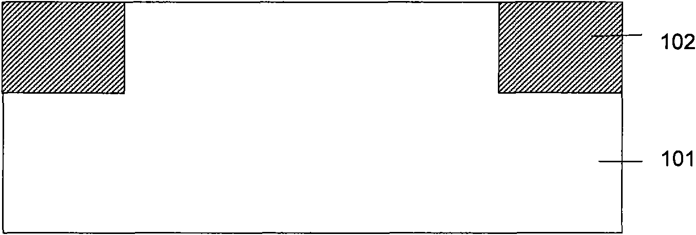
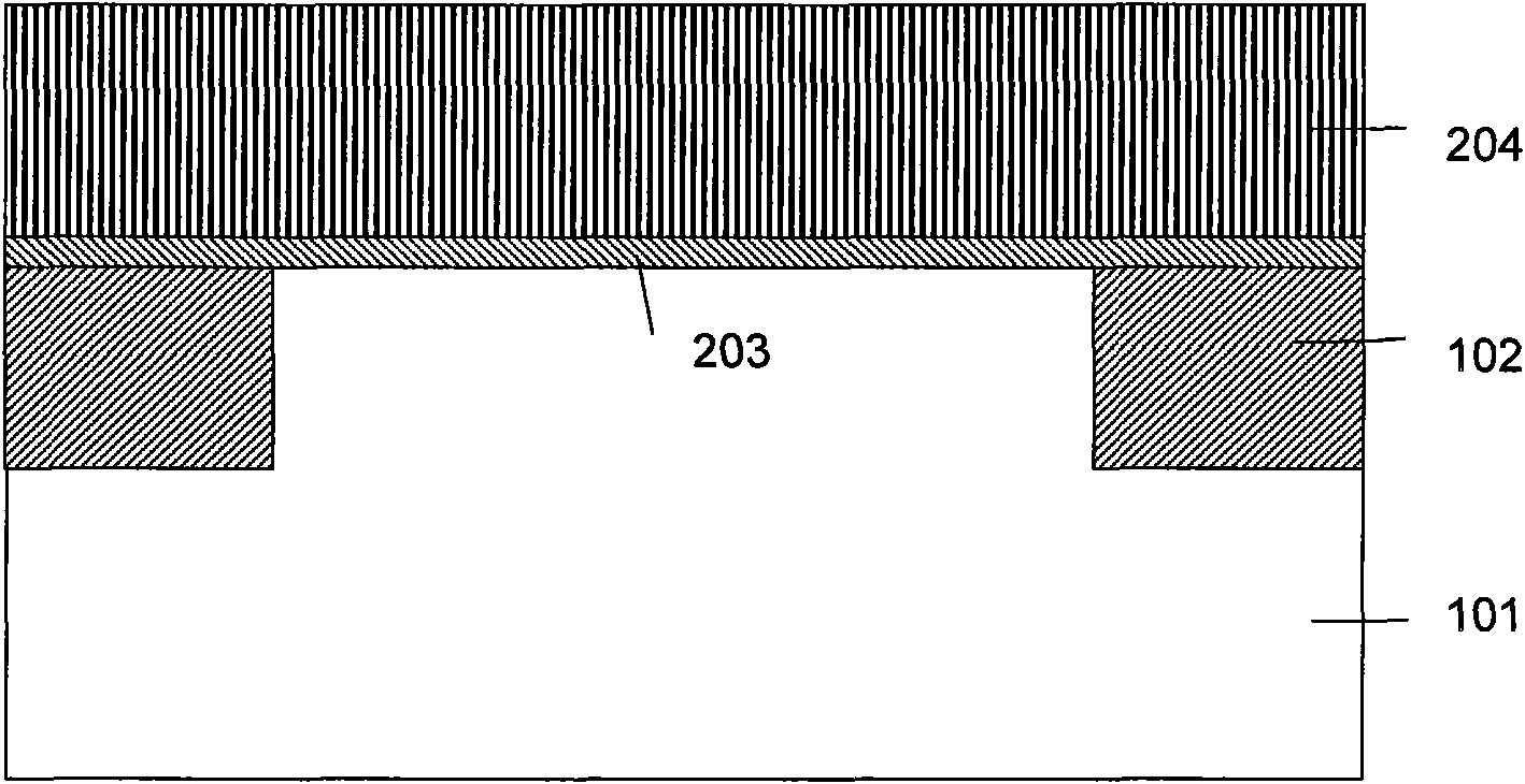
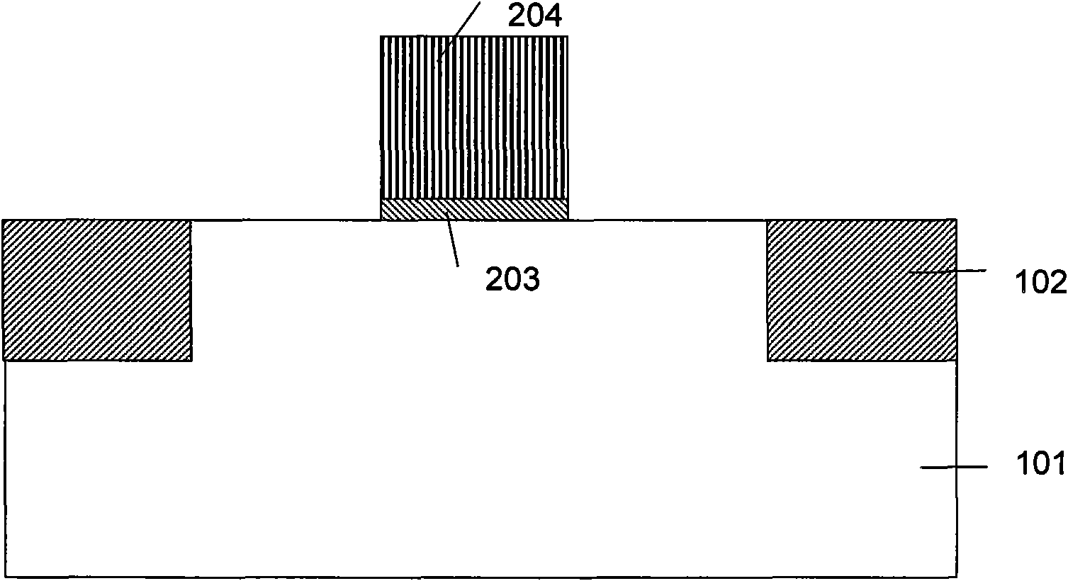
[0050] figure 1 is a schematic cross-sectional view of a semicondu...


PUM


Abstract

The invention belongs to the technical field of micro electronic appliances and in particular discloses an asymmetrical source and drain field-effect transistor and a preparation method thereof. The field-effect transistor structure comprises a semiconductor substrate, a grid structure, a source region and a drain region, wherein the source region has a mixed junction and the drain region has a PN junction respectively; the source region and the drain region are structurally asymmetrical; one of the source region and the drain region consists of the PN junction, and the other one consist of the mixed structure; and the mixed junction consists of a Schottky junction and the PN junction. The position of a doping region formed by ion injection is controlled by changing the inclination angle of the ion injection and the unique structure of the asymmetrical source and drain field-effect transistor is formed.

Description

technical field [0001] The invention belongs to the technical field of microelectronic devices, and relates to a semiconductor device and a related process preparation method, more specifically, to a field effect transistor and a preparation method thereof. Background technique [0002] MOS Field Effect Transistor (MOSFET) is the abbreviation of Metal-Oxide-Semiconductor Field Effect Transistor. It is a semiconductor device that uses electric field effect to control the current in semiconductor. polar transistor. MOS field effect transistors can be made of semiconductor silicon and germanium, and can also be made of compound semiconductor gallium arsenide and other materials. At present, silicon materials are the most used. Usually MOS field effect transistor is composed of several main parts such as semiconductor substrate, source region and drain region, gate oxide layer and gate electrode. Its basic structure is generally a four-terminal device, and its middle part is co...

Claims


Application Information

Patent Timeline
Patent Type & Authority Applications(China)
IPC IPC(8): H01L29/78H01L29/08H01L21/336H01L21/265
CPCH01L29/66659H01L21/26586H01L29/78H01L29/66643H01L21/823814H01L29/7839H01L29/66477H01L29/0847
Inventor 朴颖华葛亮吴东平张世理张卫
Owner FUDAN UNIV
Why Eureka
Try Eureka