Semiconductor component and its forming method

A semiconductor and device technology, applied in the field of semiconductor devices and their formation, can solve problems such as poor performance of semiconductor devices, and achieve the effects of increased etching degree, improved performance, and enhanced protective effect

Active Publication Date: 2017-04-05
SEMICON MFG INT (SHANGHAI) CORP +1
View PDF3 Cites 3 Cited by
  • Summary
  • Abstract
  • Description
  • Claims
  • Application Information

AI Technical Summary

Problems solved by technology

[0005] However, the performance of semiconductor devices formed in the prior art is poor

Method used


Image

  • Semiconductor component and its forming method
  • Semiconductor component and its forming method
  • Semiconductor component and its forming method

Examples


Embodiment Construction

[0022] As the feature size is further reduced, the performance of semiconductor devices formed in the prior art is poor.

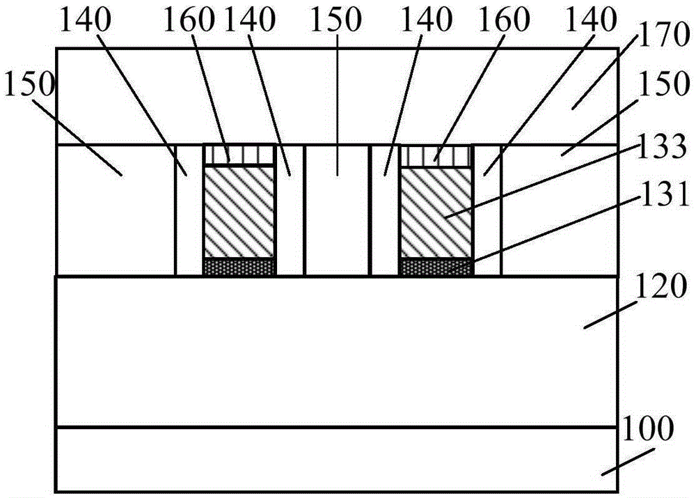
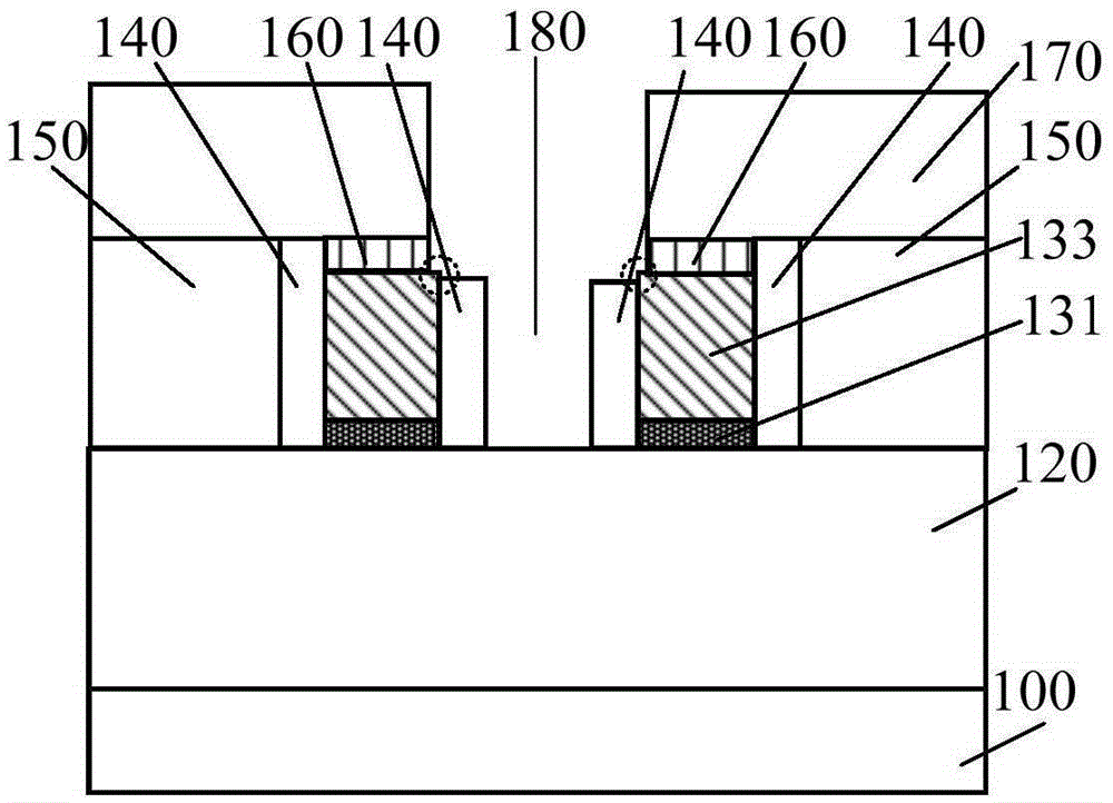
[0023] Figure 1 to Figure 3 It is a structural schematic diagram of the process of forming a semiconductor device in the prior art.

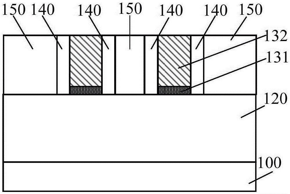
[0024] refer to figure 1 , provide a semiconductor substrate 100, the surface of the semiconductor substrate 100 has a fin 120 and a metal gate structure across the fin 120, the metal gate structure covers part of the top surface and sidewall of the fin 120, the metal gate The pole structure includes a gate dielectric layer 131 across the fin portion 120 and an initial metal gate electrode 132 covering the gate dielectric layer 131. The sidewall surfaces on both sides of the metal gate structure have sidewalls 140; the semiconductor substrate 100 and the fin portion 120 The surface has a first interlayer dielectric layer 150 covering sidewalls of the spacer 140 , and the top surface of the first interlayer dielectric laye...


PUM

PropertyMeasurementUnit
widthaaaaaaaaaa
widthaaaaaaaaaa

Abstract

The invention provides a semiconductor component and its forming method wherein the method comprises: providing a substrate whose surface is provided with a plurality of separately arranged initial metal grid electrodes, side walls at the side walls of the initial metal grid electrodes, and a first interlayer dielectric layer covering the substrate surface and the side walls at the side walls of initial metal grid electrodes with the top surface of the first interlayer dielectric layer leveled with the top surfaces of the initial metal grid electrodes; etching the initial metal grid electrodes to form target metal grid electrodes wherein the middle parts of the target metal grid electrodes are higher than the edge parts; forming a protection layer covering the target metal grid electrodes wherein the surface of the protection layer is leveled with the top surface of the first interlayer dielectric layer; forming a second interlayer dielectric layer covering the first interlayer dielectric layer, the side walls and the protection layer; and forming self-aligning contact holes that penetrate the thicknesses of the first interlayer dielectric layer and the second interlayer dielectric layer between adjacent target metal grid electrodes. The method of the invention is capable of increasing the performance of the semiconductor.

Description

technical field [0001] The invention relates to the field of semiconductor manufacturing, in particular to a semiconductor device and a forming method thereof. Background technique [0002] The MOS (metal-oxide-semiconductor) transistor is an important semiconductor device. The basic structure of the MOS transistor includes: a semiconductor substrate; a gate structure located on the surface of the semiconductor substrate; a semiconductor substrate located on one side of the gate structure The source region and the drain region in the semiconductor substrate on the other side of the gate structure. [0003] As the feature size is further reduced, the distance between adjacent gate structures is reduced, so that the process of forming contact holes for connecting the source region, the drain region and the upper metal line in the gap between the above gate structures It becomes more difficult, so the formation process of self-aligned contact holes is introduced. [0004] At ...

Claims


Application Information

Patent Timeline
Patent Type & Authority Applications(China)
IPC IPC(8): H01L29/78H01L21/336
CPCH01L29/665H01L29/66507H01L29/785H01L29/7855
Inventor 张城龙何其暘张海洋
Owner SEMICON MFG INT (SHANGHAI) CORP
Why Eureka
Try Eureka