Superconductive nanowire single-photon detector with high polarization extinction ratio
A single-photon detector and superconducting nanowire technology, which is applied in the field of light detection, can solve problems such as low polarization extinction ratio, low absorption efficiency, and influence of absorption efficiency, achieve high absorption efficiency, avoid long-distance focusing, and improve device detection efficiency effect
- Summary
- Abstract
- Description
- Claims
- Application Information
AI Technical Summary
Problems solved by technology
Method used
Image

Examples
Embodiment 1
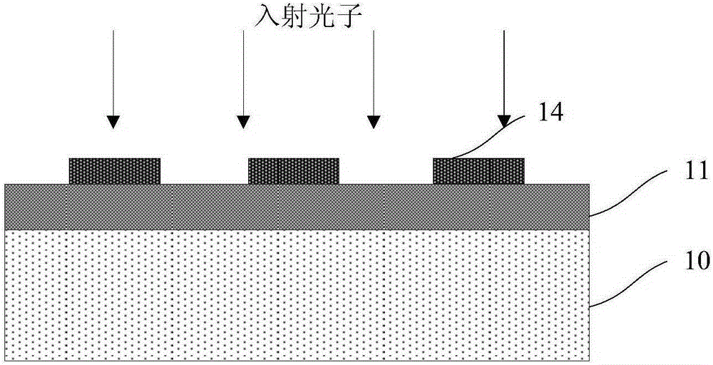
[0050] Such as image 3As shown, the present embodiment provides a high polarization extinction ratio superconducting nanowire single photon detector, including:
[0051] substrate 20;
[0052] A high reflection film 21 located on the surface of the substrate 20;
[0053] Superconducting nanowires 22, located on the surface of the high reflection film 21;
[0054] a dielectric layer 23, located on the surface of the high reflection film 21, and covering the superconducting nanowire 22;
[0055] The grating structure 24 is located on the surface of the medium layer 23 and is suitable for filtering non-target polarized light in the incident light to achieve a higher polarization extinction ratio.
[0056] As an example, the superconducting nanowire single photon detector with high polarization extinction ratio in this embodiment is a superconducting nanowire single photon detector with a front incident structure.
[0057] As an example, the substrate 20 includes a silicon su...
Embodiment 2
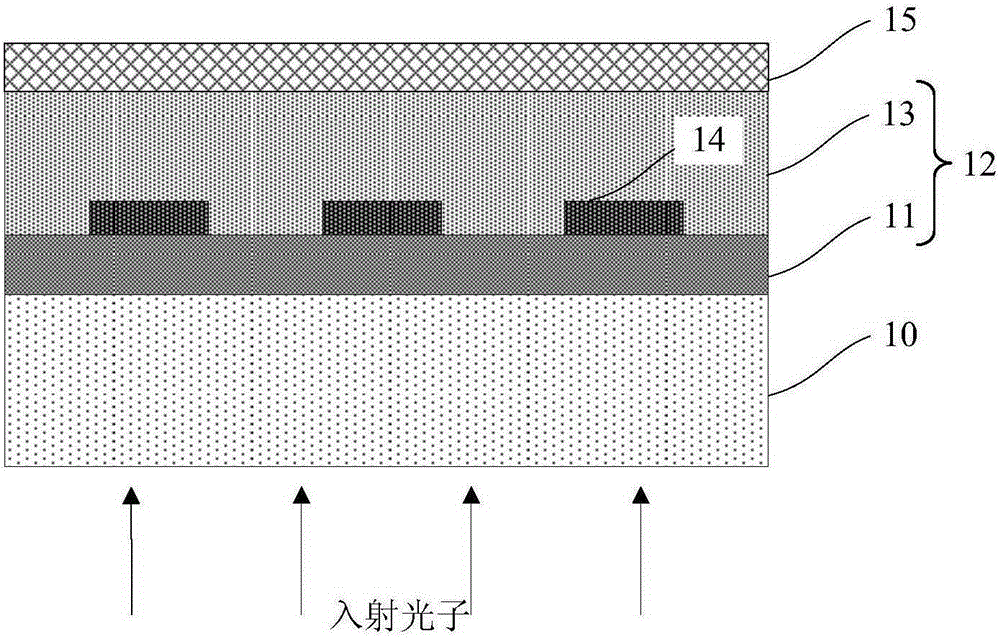
[0068] Such as Figure 4 As shown, this embodiment also provides a high polarization extinction ratio superconducting nanowire single photon detector. The difference is that: the high reflection film 21 in the first embodiment is alternately stacked SiO 2 thin film layer 211 and Si thin film layer 212; and the high reflection film 21 described in this embodiment is alternately stacked SiO 2 Thin film layer 211 with TiO 2 Thin film layer 213 . The high reflection film 21 can be the SiO 2 The thin film layer 211 is located on the surface of the substrate 20, the TiO 2 Thin film layer 213 is located on the SiO 2 Above the thin film layer 211; also can be as Figure 4 As shown in the TiO 2 The thin film layer 213 is located on the surface of the substrate 20, the SiO 2 Thin film layer 211 is located on the TiO 2 above the film layer 213.
Embodiment 3
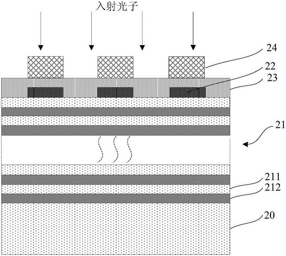
[0070] Such as Figure 5 As shown, the present embodiment provides a high polarization extinction ratio superconducting nanowire single photon detector. The basic structure of the high polarization extinction ratio superconducting nanowire single photon detector in this embodiment is basically the same as that of Embodiment 1. The difference is that the high reflection film 21 in the first embodiment is alternately stacked SiO 2 thin film layer 211 and Si thin film layer 212; and the high reflection film 21 described in this embodiment is alternately stacked SiO 2 Thin film layer 211 and Ta 2 o 5 film layer 214 . The high reflection film 21 can be the SiO 2 The thin film layer 211 is located on the surface of the substrate 20, the Ta 2 o 5 Thin film layer 214 is located on the SiO 2 Above the thin film layer 211; also can be as Figure 5 Ta 2 o 5 The thin film layer 214 is located on the surface of the substrate 20, the SiO 2 Thin film layer 211 is located on the Ta...
PUM
| Property | Measurement | Unit |
|---|---|---|
| Thickness | aaaaa | aaaaa |
| Thickness | aaaaa | aaaaa |
Abstract
Description
Claims
Application Information
 - R&D
- Intellectual Property
- Life Sciences
- Materials
- Tech Scout
- Unparalleled Data Quality
- Higher Quality Content
- 60% Fewer Hallucinations
Browse by: Latest US Patents, China's latest patents, Technical Efficacy Thesaurus, Application Domain, Technology Topic, Popular Technical Reports.
© 2025 PatSnap. All rights reserved.Legal|Privacy policy|Modern Slavery Act Transparency Statement|Sitemap|About US| Contact US: help@patsnap.com