Superconducting nanowire single photon detector based on deep silicon etching process and preparation method

A single-photon detector and superconducting nanowire technology, which is applied in the field of light detection, can solve the problems of low absorption efficiency and the influence of absorption efficiency, and achieve the effects of avoiding the influence of absorption efficiency, avoiding long-distance focusing, and high absorption efficiency

Active Publication Date: 2017-03-29
SHANGHAI INST OF MICROSYSTEM & INFORMATION TECH CHINESE ACAD OF SCI
View PDF5 Cites 41 Cited by
  • Summary
  • Abstract
  • Description
  • Claims
  • Application Information

AI Technical Summary

Problems solved by technology

[0006] In view of the above-mentioned shortcomings of the prior art, the purpose of the present invention is to provide a superconducting nanowire single photon detector based on deep silicon etching process and its preparation method, which is used to solve the problem of superconducting nanowire single photon detection in the prior art. The absorption efficiency of the detector is low, in order to solve the long-distance focusing of the back light to the NbN nanowire, a special long-focus lens is required, and the influence of the substrate Fabry-Perot cavity on the absorption efficiency, etc.

Method used


Image

  • Superconducting nanowire single photon detector based on deep silicon etching process and preparation method
  • Superconducting nanowire single photon detector based on deep silicon etching process and preparation method
  • Superconducting nanowire single photon detector based on deep silicon etching process and preparation method

Examples


Embodiment 1

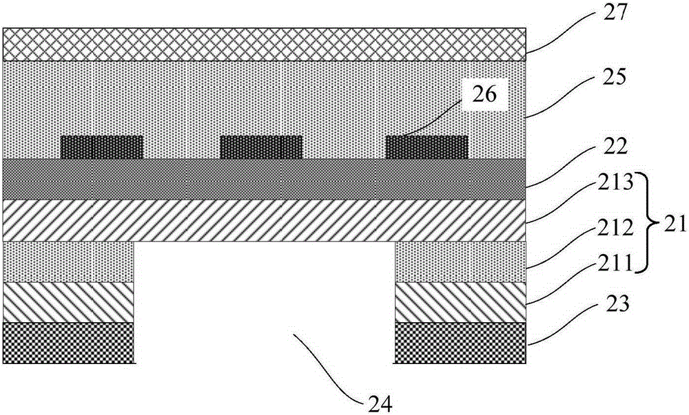
[0063] see image 3 , the present embodiment provides a superconducting nanowire single photon detector based on a deep silicon etching process, including:

[0064] SOI substrate 21, said SOI substrate 21 sequentially includes a back substrate 211, a buried oxide layer 212 and a top layer of silicon 213 from bottom to top;

[0065] The first anti-reflection layer 22 is located on the surface of the top layer silicon 213;

[0066] The second anti-reflection layer 23 is located on the surface of the back substrate 211;

[0067] a deep groove 24, penetrating through the second anti-reflection layer 23, the back substrate 211 and the buried oxide layer 212;

[0068] The optical cavity structure 25 is located on the surface of the first anti-reflection layer 22;

[0069] Superconducting nanowires 26, located between the first anti-reflection layer 22 and the optical cavity structure 25;

[0070] The mirror 27 is located on the surface of the optical cavity structure 25 .

[00...

Embodiment 2

[0079] see Figure 4 to Figure 14 , the present embodiment also provides a method for preparing a superconducting nanowire single-photon detector based on a deep silicon etching process. The method for preparing a superconducting nanowire single-photon detector based on a deep silicon etching process includes:

[0080] S1: providing an SOI substrate 21, the SOI substrate 21 sequentially includes a back substrate 211, a buried oxide layer 212 and a top layer of silicon 213 from bottom to top;

[0081] S2: forming a first anti-reflection layer 22 on the surface of the top silicon layer 213, and forming a second anti-reflection layer 23 on the surface of the back substrate 211;

[0082] S3: forming a superconducting nanowire 26 and an optical cavity structure 25 on the surface of the first anti-reflection layer 22, and the optical cavity structure 25 covers the superconducting nanowire 26;

[0083] S4: forming a mirror 27 on the surface of the optical cavity structure 25;

[00...


PUM


Abstract

The invention provides a superconducting nanowire single photon detector based on a deep silicon etching process and a preparation method. The detector comprises an SOI base which is composed of a back substrate, a buried oxygen layer and top silicon in sequence from bottom to top, a first anti-reflection layer which is disposed on the surface of the top silicon, a second anti-reflection layer which is disposed on the surface of the back substrate, a deep groove which penetrates through the second anti-reflection layer, the back substrate and the buried oxygen layer, an optical cavity structure which is disposed on the surface of the first anti-reflection layer, superconducting nanowires which are disposed between the first anti-reflection layer and the optical cavity structure, and a mirror which is disposed on the surface of the optical cavity structure. By etching the deep groove on the substrate, the distance between a coupling optical fiber and the device is narrowed, the use of a long-focus lens in the traditional back-coupling superconducting nanowire single photon detector is avoided, and alignment coupling between the MU head of an optical fiber and the device is facilitated. The problem concerning long-distance focusing in the optical cavity structure and the influence of the Fabry-Perot cavity of the susbtrate on the absorption efficiency are avoided. The absorption efficiency of target wavelength is improved. The detection efficiency of the device is improved.

Description

technical field [0001] The invention belongs to the technical field of light detection, and relates to a superconducting nanowire single-photon detector, in particular to a superconducting nanowire single-photon detector based on a deep silicon etching process and a preparation method thereof. Background technique [0002] Superconducting Nanowire Single Photon Detector (SNSPD) is a new type of single photon detection device developed in recent years, which can realize high-efficiency single photon detection from visible light to near infrared. Due to its advantages such as high quantum efficiency, low dark count, high detection rate, and low time jitter, SNSPD has been rapidly applied in applications such as quantum information technology, laser communication, satellite-to-earth ranging, bioluminescent detection, and depth imaging. [0003] SNSPD mainly uses low-temperature superconducting ultra-thin film materials, such as NbN, Nb, NbTiN, WSi, etc. The typical thickness i...

Claims


Application Information

Patent Timeline
Patent Type & Authority Applications(China)
IPC IPC(8): H01L39/02H01L39/24G01J11/00
Inventor 尤立星李浩王镇
Owner SHANGHAI INST OF MICROSYSTEM & INFORMATION TECH CHINESE ACAD OF SCI
Why Eureka
Try Eureka