Narrowband Absorbing Superconducting Nanowire Single Photon Detector

A single-photon detector and superconducting nanowire technology, which is applied in the field of light detection, can solve the problems of low absorption efficiency, performance degradation of superconducting nanowire single-photon detector, influence of absorption efficiency, etc., so as to avoid the influence of absorption efficiency, Improve the detection efficiency of the device and suppress the effect of dark counting

Active Publication Date: 2019-12-31
SHANGHAI INST OF MICROSYSTEM & INFORMATION TECH CHINESE ACAD OF SCI
View PDF4 Cites 0 Cited by
  • Summary
  • Abstract
  • Description
  • Claims
  • Application Information

AI Technical Summary

Problems solved by technology

[0008] In view of the shortcomings of the prior art described above, the purpose of the present invention is to provide a narrow-band absorption superconducting nanowire single photon detector, which is used to solve the problem of low absorption efficiency of the superconducting nanowire single photon detector in the prior art, and the substrate The influence of Fabry-Perot cavity on the absorption efficiency, and the performance degradation of superconducting nanowire single photon detector due to dark count

Method used


Image

  • Narrowband Absorbing Superconducting Nanowire Single Photon Detector
  • Narrowband Absorbing Superconducting Nanowire Single Photon Detector
  • Narrowband Absorbing Superconducting Nanowire Single Photon Detector

Examples


Embodiment 1

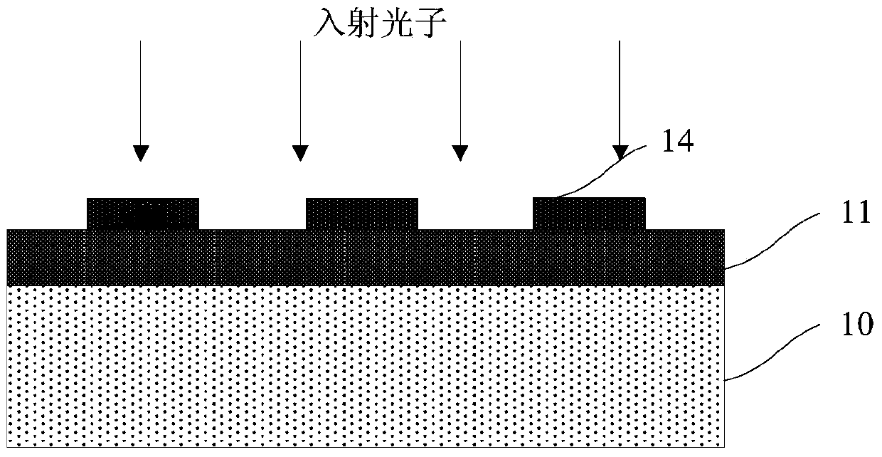
[0051] Such as image 3 As shown, this embodiment provides a narrowband absorption superconducting nanowire single photon detector, including:

[0052] substrate 20;

[0053] A high reflection film 21 located on the surface of the substrate 20;

[0054] Superconducting nanowires 22, located on the surface of the high reflection film 21;

[0055] The multilayer thin film filter 23 is located on the surface of the high reflection film 21 , and the bottom thin film layer of the multilayer thin film filter 23 covers the superconducting nanowire 22 .

[0056] As an example, the narrow-band absorbing superconducting nanowire single photon detector of this embodiment is a superconducting nanowire single photon detector with a front-incidence structure.

[0057] As an example, the substrate 20 includes a silicon substrate, an MgO substrate or a sapphire substrate, and the thickness of the substrate 20 is 300-500 microns. In this embodiment, the substrate 20 is a silicon substrate ...

Embodiment 2

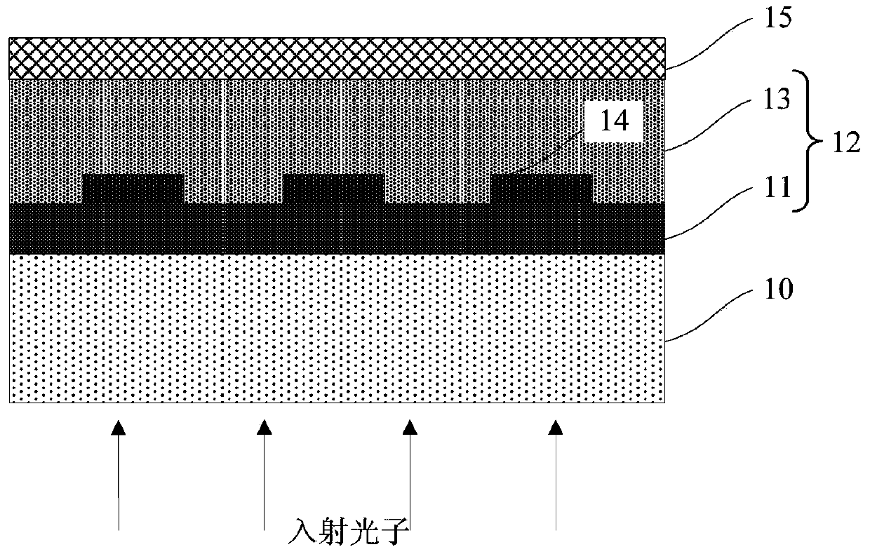
[0068] Such as Figure 5 As shown, this embodiment also provides a narrow-band absorbing superconducting nanowire single-photon detector. The basic structure of the narrow-band absorbing superconducting nanowire single-photon detector in this embodiment is basically the same as that in Embodiment 1. The difference between the two is : The multilayer thin film filter 23 described in Embodiment 1 is an alternately stacked SiO 2 Thin film layer 211 with TiO 2 thin film layer 213; and the multilayer thin film filter 23 described in this embodiment is an alternately stacked SiO 2 Thin film layer 211 and Ta 2 o 5 film layer 214 . The multilayer thin film filter 23 can be the SiO 2 The thin film layer 211 is located on the surface of the high reflection film 21, and the Ta 2 o 5 Thin film layer 214 is located on the SiO 2 Above the thin film layer 211; also can be as Figure 5 Ta 2 o 5 The thin film layer 214 is located on the surface of the high reflection film 21, and th...

Embodiment 3

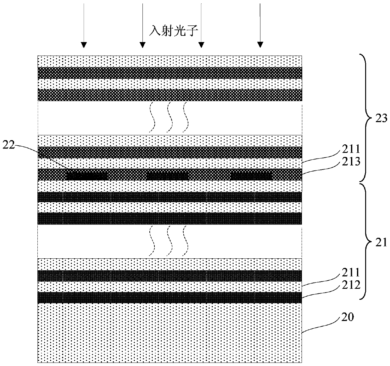
[0070] Such as Figure 6 As shown, this embodiment provides a narrow-band absorbing superconducting nanowire single-photon detector. The basic structure of the narrow-band absorbing superconducting nanowire single-photon detector in this embodiment is basically the same as that of Embodiment 1. The difference between the two is: The high reflection film 21 described in Example 1 is alternately stacked SiO 2 thin film layer 211 and Si thin film layer 212, and the high reflection film 21 described in this embodiment is an alternately stacked SiO 2 Thin film layer 211 with TiO 2 Thin film layer 213; the multilayer thin film filter 23 described in embodiment 1 is SiO stacked alternately 2 Thin film layer 211 with TiO 2 thin film layer 213; and the multilayer thin film filter 23 described in this embodiment is an alternately stacked SiO 2 thin film layer 211 and Si thin film layer 212 . The high reflection film 21 can be the SiO 2 The thin film layer 211 is located on the sur...


PUM


Abstract

The invention provides a narrow-band absorption superconducting nanowire single photo detector. The narrow-band absorption superconducting nanowire single photo detector comprises a substrate, a high-reflective film, a superconducting nanowire and a multi-layer thin film filter, wherein the high-reflective film is arranged on a surface of the substrate, the superconducting nanowire is arranged on a surface of the high-reflective film, and the multi-layer thin film filter is arranged on the surface of the high-reflective film, and a bottom thin film layer of the multi-layer thin film filter wraps the superconducting nanowire. In the narrow-band absorption superconducting nanowire single photo detector, the superconducting nanowire is prepared based on the high-reflective film substrate, light can directly irradiate the superconducting nanowire through front-surface coupling, the problem of remote focusing in an optical cavity structured superconducting nanowire single photo detector can be avoided, the influence of a substrate Fabry-Perot cavity on absorption efficiency is further prevented, the superconducting nanowire single photo detector has relatively high absorption efficiency on a target wavelength, and the detection efficiency of the device is effectively improved; and meanwhile, the multi-layer thin film filter on the nanowire has a non-target wavelength filtering function, stray light in incident light can be filtered, and dark count caused by black-body radiation is further effectively suppressed.

Description

technical field [0001] The invention belongs to the technical field of light detection, and relates to a superconducting nanowire single-photon detector, in particular to a narrow-band absorption superconducting nanowire single-photon detector. Background technique [0002] Superconducting Nanowire Single Photon Detector (SNSPD) is a new type of single photon detection device developed in recent years, which can realize high-efficiency single photon detection from visible light to near infrared. Due to its advantages such as high quantum efficiency, low dark count, high detection rate, and low time jitter, SNSPD has been rapidly applied in applications such as quantum information technology, laser communication, satellite-to-earth ranging, bioluminescent detection, and depth imaging. [0003] SNSPD mainly uses low-temperature superconducting ultra-thin film materials, such as NbN, Nb, NbTiN, WSi, etc. The typical thickness is about 5-10nm, and the device usually adopts a me...

Claims


Application Information

Patent Timeline
Patent Type & Authority Patents(China)
IPC IPC(8): H01L39/00H01L39/02
Inventor 李浩尤立星王镇
Owner SHANGHAI INST OF MICROSYSTEM & INFORMATION TECH CHINESE ACAD OF SCI
Why Eureka
Try Eureka