Method for identifying a short circuit in a first light emitting diode element, and optoelectronic subassembly

A technology of light-emitting diodes and optoelectronics, applied in diode testing, electroluminescent light sources, short-circuit testing, etc., can solve problems such as high current density, electrode melting, heating, etc., and achieve the effect of simply identifying short-circuits

Active Publication Date: 2017-04-19
OSRAM OLED
View PDF8 Cites 3 Cited by
  • Summary
  • Abstract
  • Description
  • Claims
  • Application Information

AI Technical Summary

Problems solved by technology

The current density is therefore significantly too high, so that these locations can heat up very strongly depending on the configuration of the surfaces
This can cause electrodes to melt, cause dark spots in the glow image, cause a completely dark OLED, and / or simply cause places on the OLED to get very hot

Method used


Image

  • Method for identifying a short circuit in a first light emitting diode element, and optoelectronic subassembly
  • Method for identifying a short circuit in a first light emitting diode element, and optoelectronic subassembly
  • Method for identifying a short circuit in a first light emitting diode element, and optoelectronic subassembly

Examples


Embodiment Construction

[0052] In the ensuing detailed description, reference is made to the accompanying drawings, which form a part hereof, and in which specific embodiments are shown for purposes of illustration, in which specific The present invention can be implemented in an embodiment. In this respect, directional terms such as "above", "below", "in front of", "behind", "in front of", "behind" etc. are used with respect to the orientation of the depicted figures Wait. Because components of an embodiment may be positioned in a number of different orientations, the directional terms are used for clarification and are not limiting in any way. It is easy to understand that other embodiments can be used and structural or logical changes can be made without departing from the protection scope of the present invention. It is easy to understand that: unless otherwise specified, the features of different embodiments described here can be combined with each other. Therefore, the ensuing detailed descr...


PUM


Abstract

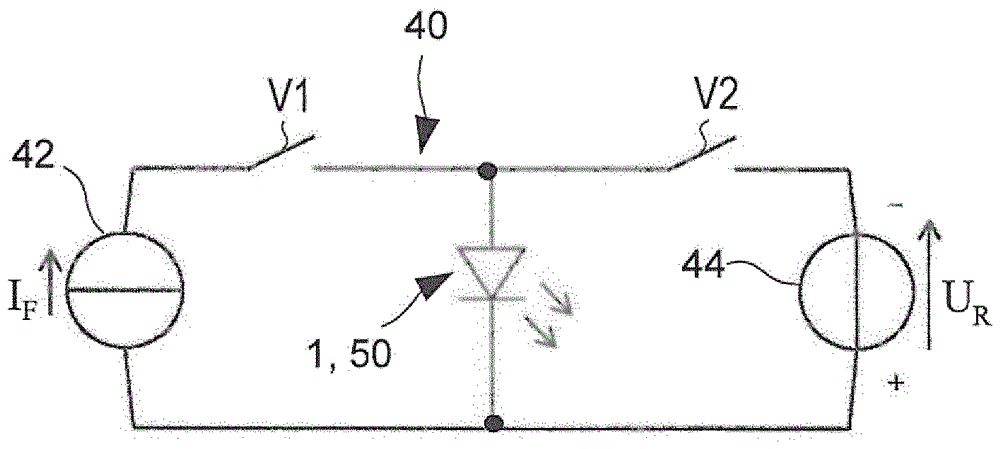
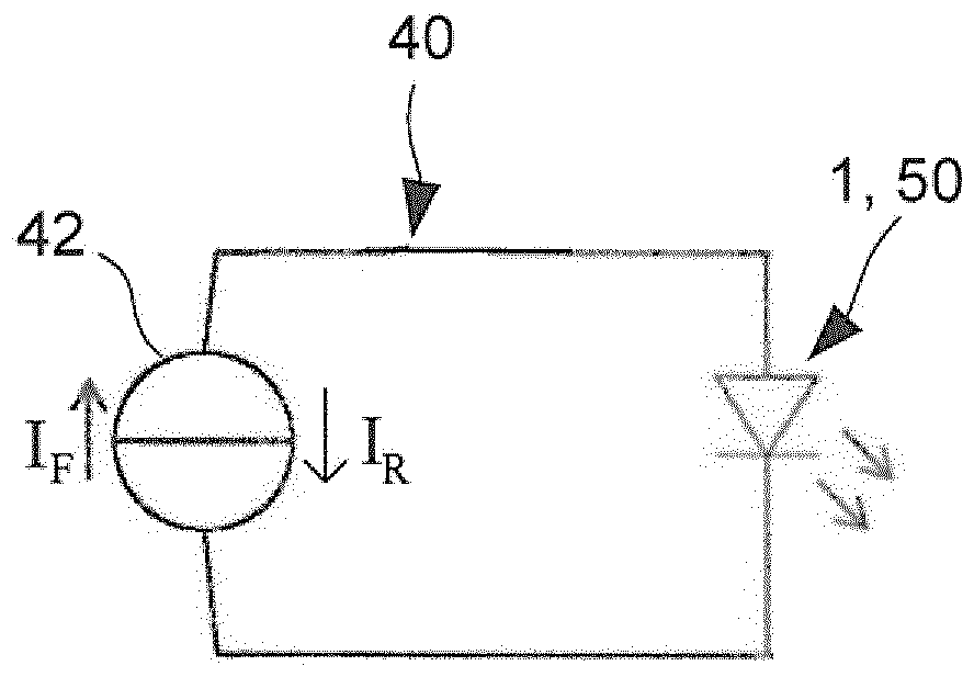
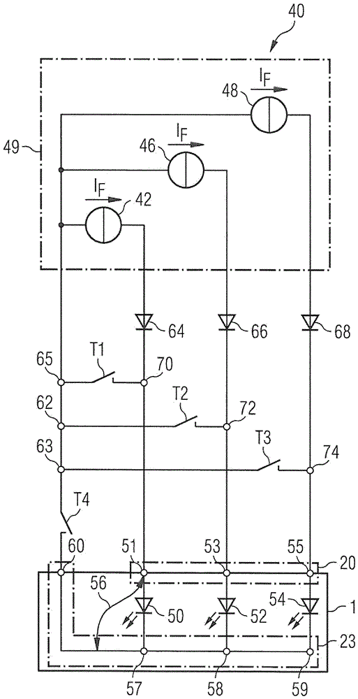
Various exemplary embodiments relate to a method for identifying a short circuit in a first light emitting diode element (50). In said method, the first light emitting diode element (50) is operated in the reverse mode. Verification is made as to whether an electric current (IR) flows in the reverse direction across the light emitting diode element (50), and the short circuit is identified if said verification indicates that the current (IR) flows in the reverse direction and is greater than a given leakage current.

Description

technical field [0001] The invention relates to a method for detecting a short circuit in a first light-emitting diode element and to an optoelectronic component. Background technique [0002] The light-emitting optoelectronic component can be, for example, a light-emitting diode (LED) or an organic light-emitting diode (OLED). OLEDs can have an anode and a cathode, the cathode having an organic functional layer system between the anode and the cathode. The organic functional layer system can have: one or more emitter layers, in which electromagnetic radiation is generated; a charge carrier pair generating layer structure, which is respectively composed of Two or more carrier pair generating layers ("charge generating layers", CGLs) for generating carrier pairs; and one or more electron blocking layers, also known as hole a "hole transport layer" (HTL); and one or more hole-blocking layers, also known as "electron transport layers" (ETL), in order to rectify (richten) the ...

Claims


Application Information

Patent Timeline
Patent Type & Authority Applications(China)
IPC IPC(8): G01R31/26H05B33/08H05B44/00
CPCG01R31/2635H05B45/58H05B45/46H05B45/60Y02B20/30H05B45/52G01R31/52
Inventor K.雷高
Owner OSRAM OLED
Why Eureka
Try Eureka