Electrostatic protection structure

An electrostatic protection and circuit protection technology, applied in the field of electrostatic protection structure, can solve the problems of application restrictions, inappropriate installation of metal protective nets, electrostatic damage of electronic components, etc., and achieve the effect of avoiding electrostatic damage

Active Publication Date: 2017-04-26
UNIVERSAL SCIENTIFIC INDUSTRIAL (SHANGHAI) CO LTD
View PDF6 Cites 12 Cited by
  • Summary
  • Abstract
  • Description
  • Claims
  • Application Information

AI Technical Summary

Problems solved by technology

And when people use these mobile electronic products, static electricity (ESD) may be generated due to factors such as contact, separation, friction or induction between the human body's own actions and other objects in a dry climate, and the arc generated by static electricity will pass through the electronic Openings or through-holes in the product's casing and circuit substrate directly enter, so electronic components may be damaged by electrostatic discharge arcs passing through said openings or through-holes
[0007] However, in the existing ESD protection structure, the ESD protection electronic components are connected in series on the connection lines of the electronic components, so it can only prevent the electrostatic current conducted from the circuit substrate from damaging the electronic components. If the ESD arc is directly When passing through openings or through holes of the casing or circuit substrate, electronic components may still be directly exposed to electrostatic arcs and be damaged by static electricity
[0008] In order to prevent the electrostatic arc passing through the opening or perforation of the casing or circuit substrate from damaging the electronic components, most of the existing mobile electronic products adopt a metal protective net outside the opening or through hole of the casing. Setting a protective net in the opening will increase the size of the electronic product, and it is not suitable to install a metal protective net for the miniature microphone component, so the application of this kind of electrostatic protection structure is limited

Method used


Image

  • Electrostatic protection structure
  • Electrostatic protection structure
  • Electrostatic protection structure

Examples


Embodiment Construction

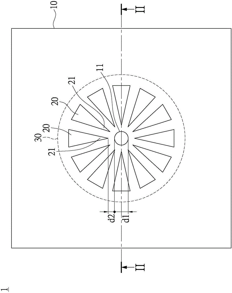
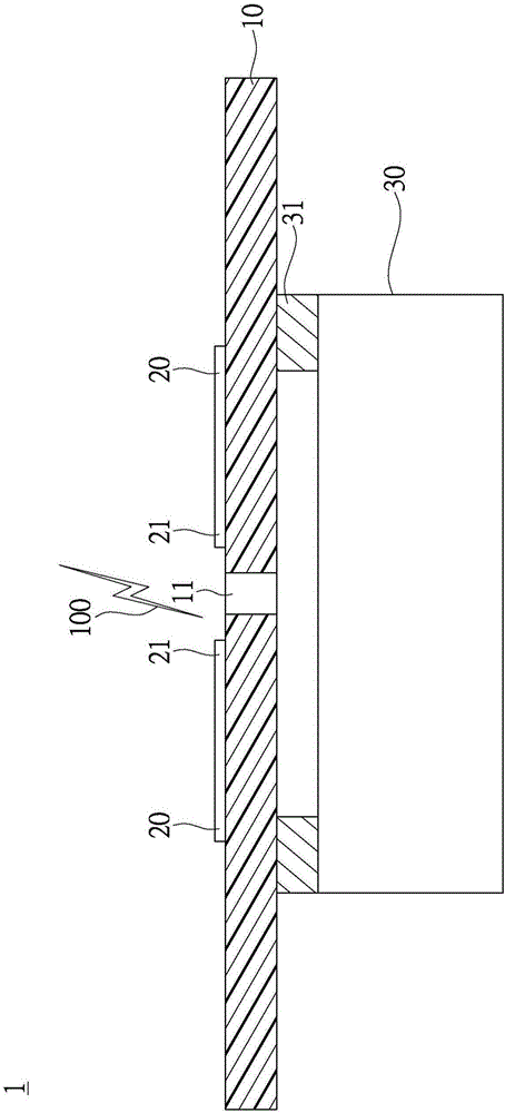
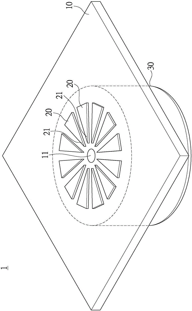
[0022] The technology of the present invention is an electrostatic protection structure 1 applied to electrostatic sensitive electronic components on electronic products. The electrostatic protection structure 1 of the present invention includes a plurality of protective conductors 20, and Figure 1 to Figure 3 Shown is a schematic structural view of a circuit substrate 10 and an electronic component 30 of an electronic product using the electrostatic protection structure 1 of the present invention. Wherein, the electronic component 30 can be a surface-mounted (SMT) electronic component, and is fixed on a surface of the circuit substrate 10 by soldering pads 31, and the circuit substrate 10 can be a multi-layer printed circuit board, and The circuit substrate 10 is provided with an opening 11 corresponding to the electronic component 30 , so the positions of the electronic component 30 and the opening 11 overlap each other and will not be blocked by the circuit substrate 10 . ...


PUM


Abstract

The invention discloses an electrostatic protection structure which comprises a circuit substrate and a plurality of protective conductors. The circuit substrate is provided with an opening. The plurality of protective conductors are arranged on one side face of the circuit substrate and are adjacent to the periphery of the opening. Each of the protective conductors comprises a tip part and is arranged at the periphery of the opening in a direction that the tip part faces the center of the opening, and each of the protective conductors is electrically connected to the grounding line of the circuit substrate. The protective conductors can guide an electrostatic discharge arc to face the protective conductors, thus a condition that the electrostatic discharge arc passes the opening of the circuit substrate so as to avoid the damage to electronic components adjacent to the opening by static electricity.

Description

technical field [0001] The invention relates to an electrostatic protection structure, in particular to an electrostatic protection structure for preventing electrostatic discharge arcs from passing through openings of mobile electronic products, so as to prevent electronic components from being damaged by static electricity. Background technique [0002] With the rapid development of mobile communication technology, mobile electronic products such as mobile phones, tablet computers, smart watches, and portable media players are becoming more and more popular. Due to the convenience, compactness and powerful functions of these products, they have become indispensable in our daily work. important communication tool. [0003] Generally speaking, sound energy conversion components such as microphones and speakers are installed on the mobile electronic products as audio input and output devices of the mobile electronic products. In addition, due to the gradual diversification o...

Claims


Application Information

Patent Timeline
Patent Type & Authority Applications(China)
IPC IPC(8): H05K1/02
CPCH05K1/0259H05K2201/09209
Inventor 刘彦中张致纲
Owner UNIVERSAL SCIENTIFIC INDUSTRIAL (SHANGHAI) CO LTD
Why Eureka
Try Eureka