Thin film transistor and making method thereof

A technology of thin film transistors and manufacturing methods, applied in the field of thin film transistors and their manufacturing, capable of solving problems such as unfavorable development of thin-type displays and increase of overall thickness, and achieving the effect of being conducive to the development of thin-type displays and reducing overall thickness

Active Publication Date: 2017-05-03
HONG FU JIN PRECISION IND (SHENZHEN) CO LTD +1
View PDF4 Cites 3 Cited by
  • Summary
  • Abstract
  • Description
  • Claims
  • Application Information

AI Technical Summary

Problems solved by technology

However, for the thin film transistor with this structure, when the channel layer needs to meet a certain thickness, the additional ohmic contact layer will increase the overall thickness of the thin film transistor, which is not conducive to the development of thin displays.

Method used


Image

  • Thin film transistor and making method thereof
  • Thin film transistor and making method thereof
  • Thin film transistor and making method thereof

Examples


Embodiment Construction

[0018] The embodiments of the present invention will be further described in detail below in conjunction with the accompanying drawings.

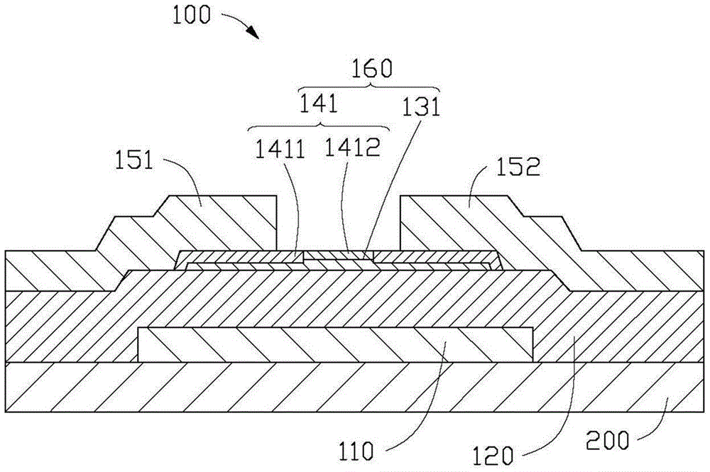
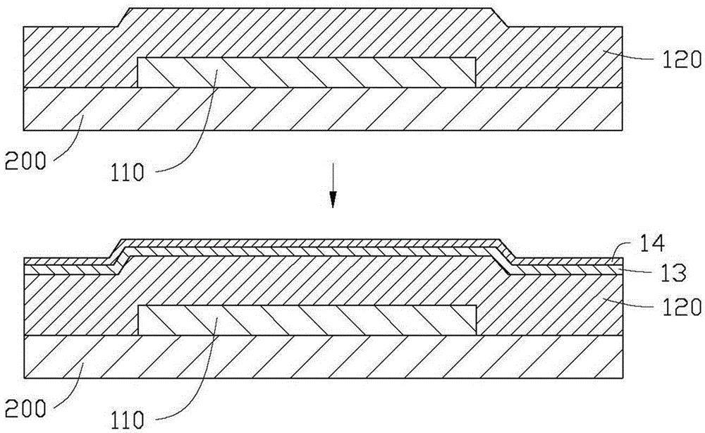
[0019] see figure 1 , a cross-sectional view of the structure of the thin film transistor 100 provided by the present invention. The TFT 100 is formed on a substrate 200 , and the TFT 100 includes a gate 110 , a gate insulating layer 120 , an intrinsic amorphous silicon layer 160 , a source 151 and a drain 152 . The gate 110 is located on the substrate 200, the gate insulating layer 120 covers the substrate 200 and the gate 110, and the intrinsic amorphous silicon layer 160 is disposed on the side of the gate insulating layer 120 away from the substrate 200. and located at a position corresponding to the gate 110 . The gate insulating layer 120 is used to insulate the gate 110 from the intrinsic amorphous silicon layer 160 , the source 151 and the drain 152 . The intrinsic amorphous silicon layer 160 further includes a first layer 131 an...


PUM


Abstract

A thin film transistor comprises a gate, a gate insulation layer, an intrinsic amorphous silicon layer, a source, and a drain. The gate insulation layer is arranged between the gate and the intrinsic amorphous silicon layer to insulate the gate and the intrinsic amorphous silicon layer from each other. The intrinsic amorphous silicon layer includes a first layer and a second layer covering the first layer. The second layer includes a non-doped region and a doped region at the two sides of the non-doped region. Both the source and the drain are in contact with the doped region. The non-doped region and at least part of the doped region are exposed between the source and the drain.

Description

technical field [0001] The invention relates to a thin film transistor and a manufacturing method thereof. Background technique [0002] Thin film transistors are used in displays and are usually used as switches for charging or discharging storage capacitors. A common thin film transistor includes a gate, a gate insulating layer, a channel layer, an ohmic contact layer, a source and a drain. Gates are used to open or close the passage of electrons in the channel layer. The gate insulating layer covers the gate to insulate the gate and the channel layer from each other, and the ohmic contact layer is disposed on the channel layer. The source and the drain are respectively arranged at two ends of the ohmic contact layer, and the ohmic contact layer between the source and the drain will be etched away to expose the channel layer. Among them, the channel layer between the source and drain electrodes is used as a back channel, and needs to meet a certain thickness to provide ...

Claims


Application Information

Patent Timeline
Patent Type & Authority Applications(China)
IPC IPC(8): H01L29/786H01L29/06H01L29/66
CPCH01L29/0684H01L29/66765H01L29/78669
Inventor 安生健二
Owner HONG FU JIN PRECISION IND (SHENZHEN) CO LTD
Why Eureka
Try Eureka