Wafer etching device and method

A technology for etching devices and wafers, which is applied in the manufacture of electrical components, electrical solid devices, semiconductor/solid devices, etc., can solve the problems of reduction and no obvious improvement in the yield rate of integrated circuits, achieve good isolation performance, and avoid trenches Decrease in isolation performance and improve yield

Active Publication Date: 2017-05-10
BEIJING NAURA MICROELECTRONICS EQUIP CO LTD
View PDF2 Cites 8 Cited by
  • Summary
  • Abstract
  • Description
  • Claims
  • Application Information

AI Technical Summary

Problems solved by technology

[0004] However, during the actual testing and application of the above-mentioned solution for improving etching uniformity, the inventors of the present invention found that the yield rate of integrated circuits etched by using the solution for improving etching uniformity was not significantly improved, and even sometimes lower

Method used


Image

  • Wafer etching device and method
  • Wafer etching device and method
  • Wafer etching device and method

Examples


Embodiment Construction

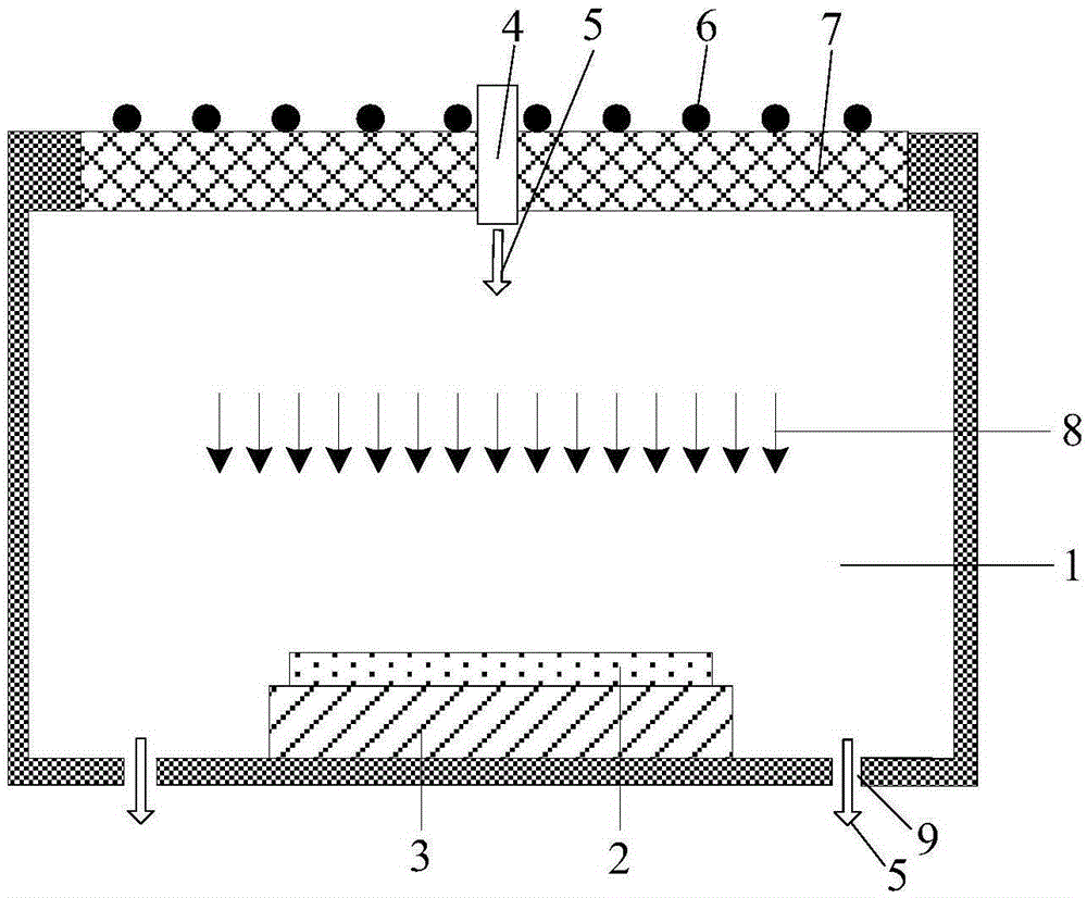
[0040] As described in the background art, in the prior art, the etching uniformity is improved by rotating the placing table 3 or setting a rotating shaft under the wafer 2 to drive the wafer 2 to rotate, but this solution does not make the integrated circuit good. The rate has been significantly improved, and sometimes even the yield rate of integrated circuits will be reduced. The inventor of the present invention finds through a large amount of research and experiment, and the main cause of above-mentioned problem is:

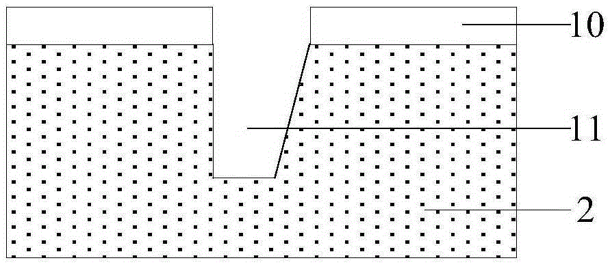
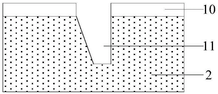
[0041] Such as Figure 2a with Figure 2b As shown, in the prior art, the placement table 3 can only drive the wafer 2 to rotate in one direction, that is, only rotate clockwise or only counterclockwise, because the etching process is to transfer the pattern on the mask 10 to the wafer 2, so the unidirectional rotation of the wafer 2 will deflect the pattern transmission at a certain angle, and finally cause the left and right side walls of the trench 11 ...


PUM


Abstract

The invention provides a wafer etching device and method, and relates to the technical field of semiconductors, wherein the device and method are used for improving the etching uniformity of a wafer, and improving the yield of an integrated circuit. The device comprises an etching cavity and a placement platform which is disposed in the etching cavity and can rotate. The placement platform is used for bearing the wafer, and at least rotates clockwise for one circle and anticlockwise for one circle in the etching process of the wafer. The device provided by the invention is used for the etching of the device.

Description

technical field [0001] The invention relates to the technical field of semiconductors, in particular to a wafer etching device and an etching method. Background technique [0002] Inductively coupled plasma etching is currently a major etching method used in the field of integrated circuit manufacturing, and its basic process is as follows: figure 1 As shown, a patterned mask is formed on the wafer 2, and then the wafer 2 is placed on the placement table 3 in the etching chamber 1; the etching gas 5 is passed into the etching chamber through the gas delivery structure 4 In the body 1, and on the upper radio frequency electrode 6 and the lower radio frequency electrode (set on the placement platform 3, figure 1 (not shown in ), respectively add radio frequency power to generate arc discharge, and ionize part of the etching gas to generate ions, electrons and free radicals. This gas-phase substance composed of partially ionized gas is called plasma 8; plasma 8 Under the acti...

Claims


Application Information

Patent Timeline
Patent Type & Authority Applications(China)
IPC IPC(8): H01L21/67H01L21/683
CPCH01L21/67069H01L21/683H01L2221/683
Inventor 陈永远
Owner BEIJING NAURA MICROELECTRONICS EQUIP CO LTD
Why Eureka
Try Eureka