Stepped upper electrode for plasma processing uniformity

A plasma and plasma chamber technology, applied in the field of stepped upper electrodes for uniform plasma processing, can solve the problem of reducing the etching rate near the edge of the processed substrate

Inactive Publication Date: 2006-01-18
LAM RES CORP
View PDF16 Cites 9 Cited by
  • Summary
  • Abstract
  • Description
  • Claims
  • Application Information

AI Technical Summary

Problems solved by technology

Therefore, the use of conventional parallel plate reactors during plasma etch reduces the etch rate near the edge of the substrate being processed

Method used


Image

  • Stepped upper electrode for plasma processing uniformity
  • Stepped upper electrode for plasma processing uniformity
  • Stepped upper electrode for plasma processing uniformity

Examples


Embodiment Construction

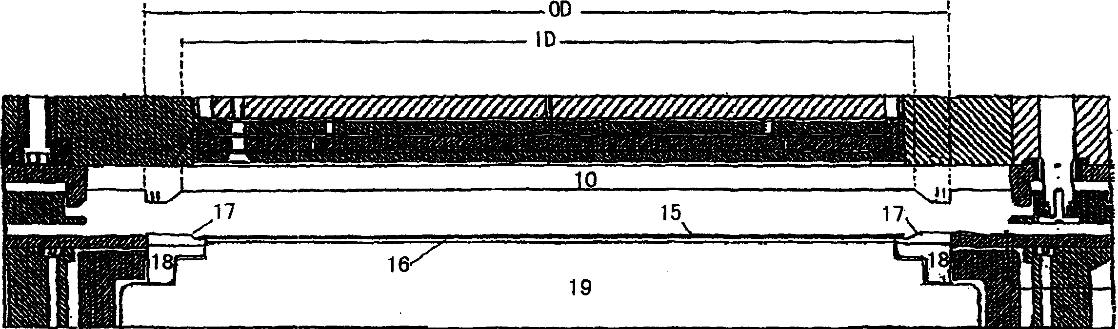
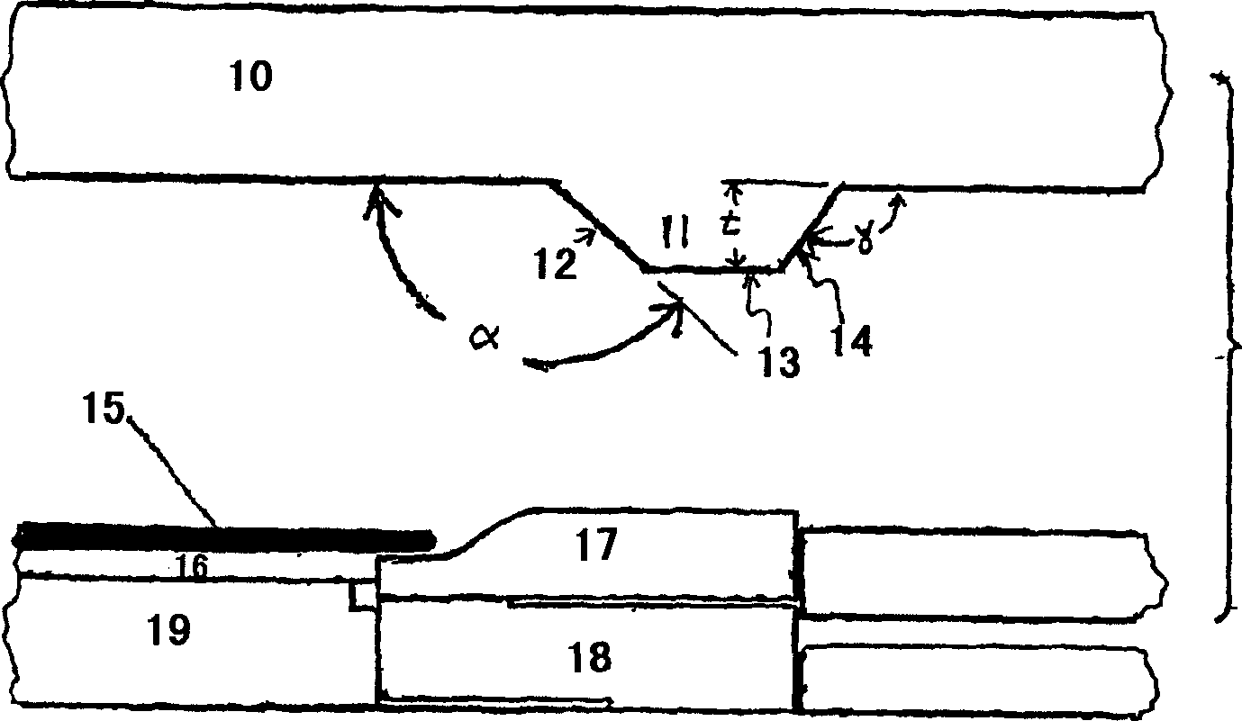
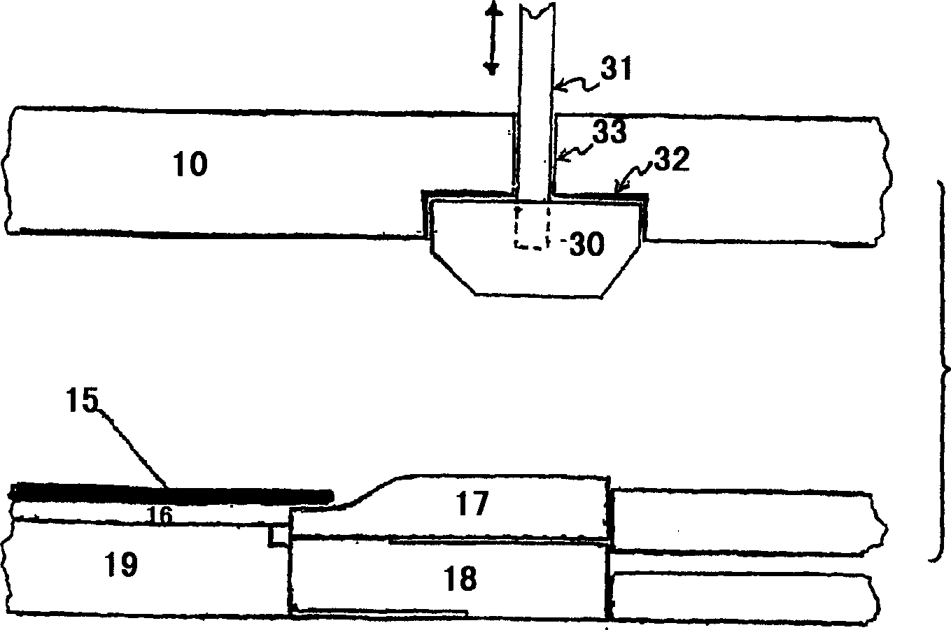
[0033] The present invention provides a novel arrangement for improving uniformity during plasma processing of semiconductor substrates such as silicon wafers, flat panel display substrates, and the like. This improved plasma processing can be achieved by adjusting the plasma density on the peripheral region of the substrate being processed. Uniformity can be improved by using stepped electrodes. Further improvements can be made by changing the material, shape and / or power of the hot edge ring (HER) surrounding the substrate being processed.

[0034] The stepped electrode according to the present invention can be applied to the plasma etching process to increase the plasma density near the edge of the wafer in the parallel plate plasma reaction chamber, so as to obtain a more uniform etching rate on the substrate. Although the invention has been described based on the advantages of a plasma etch process, the invention can also be used in other applications requiring a uniform...


PUM


Abstract

A plasma discharge electrode having a front surface with a central portion thereof including gas outlets discharging a process gas which forms a plasma and a peripheral portion substantially surrounding the gas outlets. The peripheral portion has at least one step for controlling a density of the plasma formed by the electrode. The electrode can be used as the grounded upper electrode in a parallel plate plasma processing apparatus such as a plasma etching apparatus. The geometric features of the step and of a corresponding edge ring on the lower electrode can be varied to achieve the desired etch rate profile across a wafer surface.

Description

technical field [0001] The present invention relates generally to methods of etching using high energy radiation or plasma, and more particularly to a method and apparatus for controlling the etch rate at the edge of a wafer during the manufacture of integrated semiconductor circuits. Background technique [0002] Since the mid-1960s, integrated semiconductor circuits have gradually become the main components of most electronic systems. These miniaturized electronic devices can contain thousands of transistors and other circuits that make up the memory and logic subsystems of a microcomputer's central processing unit. The low cost, high reliability, and speed of operation of these computer chips have made them a ubiquitous feature of modern digital electronics. [0003] The fabrication process of integrated circuit chips typically begins with a thin, polished slice of a substrate of high-purity, single-crystal semiconductor material called a "wafer." Each wafer undergoes a...

Claims


Application Information

Patent Timeline
Patent Type & Authority Applications(China)
IPC IPC(8): H01J37/32H01L21/3065
CPCH01J37/32009H01J37/3244Y10T156/10H01J37/32
Inventor 拉金德尔·德辛德萨穆昆德·斯利尼瓦桑艾伦·爱普勒埃里克·兰兹
Owner LAM RES CORP
Why Eureka
Try Eureka