Array substrate and display device

A technology for array substrates and display devices, which is applied in printed circuits, circuits, and electric solid-state devices, and can solve problems such as large resistance, different signals, and influence on display uniformity

Active Publication Date: 2017-05-10
BOE TECH GRP CO LTD +1
View PDF5 Cites 21 Cited by
  • Summary
  • Abstract
  • Description
  • Claims
  • Application Information

AI Technical Summary

Problems solved by technology

At present, the resistance of the high-level signal line and the low-level signal line is large, which causes the signals received by the pixel circuits in different regions to be different, so that the brightness of the organic light-emitting units in different regions is different, thereby affecting the uniformity of display.

Method used


Image

  • Array substrate and display device
  • Array substrate and display device
  • Array substrate and display device

Examples


Embodiment Construction

[0032] Specific embodiments of the present invention will be described in detail below in conjunction with the accompanying drawings. It should be understood that the specific embodiments described here are only used to illustrate and explain the present invention, and are not intended to limit the present invention.

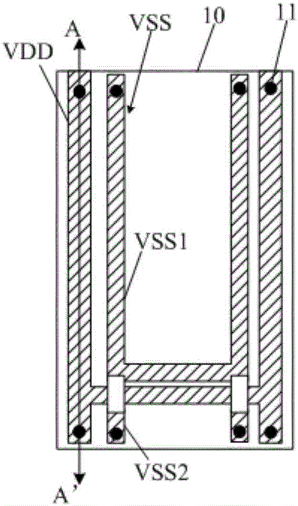
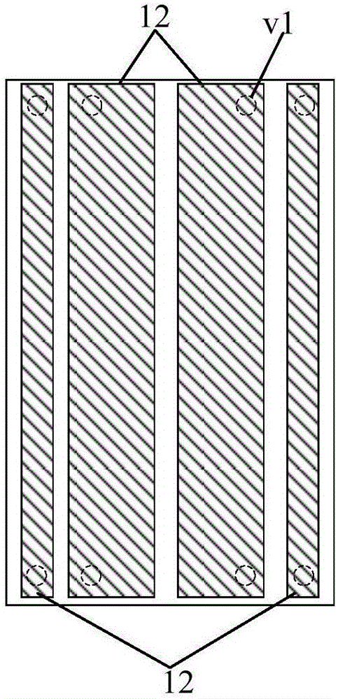
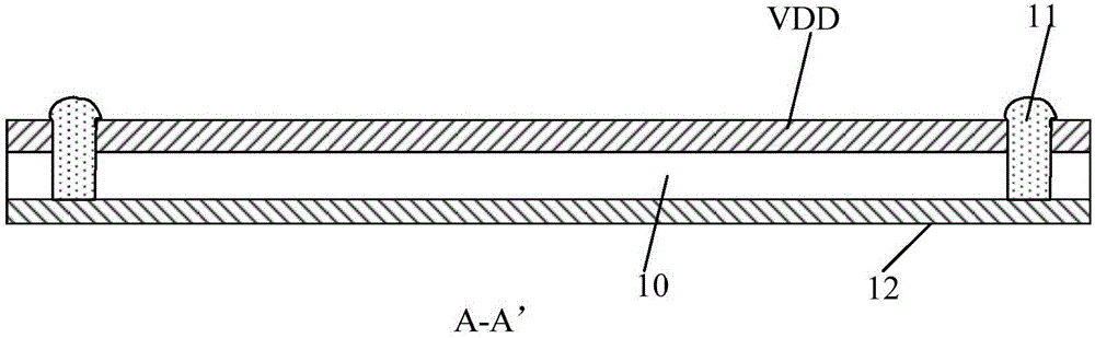
[0033] As an aspect of the present invention, an array substrate is provided, combined with Figure 1a to Figure 3b As shown, the array substrate includes a substrate 10 and signal lines (such as Figure 1a The high-level signal line VDD and the low-level signal line VSS), the substrate 10 is also provided with a conductive member 12 corresponding to the signal line, and the signal line is connected in parallel with the corresponding conductive member 12. Different signal lines The corresponding conductive elements 12 are insulated from each other. Wherein, the parallel connection of the signal line and the corresponding conductive member 12 means that at least...


PUM


Abstract

The invention provides an array substrate. The array substrate comprises a substrate and signal wires, wherein the signal wires are arranged on the substrate; conductive parts, corresponding to the signal wires, are further arranged on the substrate; the signal wires are in parallel connection with the corresponding conductive parts; and the conductive parts corresponding to different signal wires are insulated and are spaced. Correspondingly, the invention further provides a display device. According to the array substrate and the display device provided by the invention, the resistance of the signal wires can be reduced; and thus, the display effect is improved.

Description

technical field [0001] The present invention relates to the field of display technology, in particular to an array substrate and a display device. Background technique [0002] In an organic electroluminescence (Organic Light-Emitting Diode, OLED) display device, an organic light-emitting unit and a pixel circuit for providing a driving current for the organic light-emitting unit are arranged in each pixel, and a high voltage is arranged in the pixel circuit. The flat signal terminal and the low level signal terminal are used to receive the high level signal and the low level signal respectively, and the high level signal and the low level signal are provided by the high level signal line and the low level signal line respectively. At present, the resistance of the high-level signal line and the low-level signal line is large, which causes the signals received by the pixel circuits in different regions to be different, so that the brightness of the organic light-emitting uni...

Claims


Application Information

Patent Timeline
Patent Type & Authority Applications(China)
IPC IPC(8): H01L27/32
CPCH10K59/1315H10K59/131H01L27/124Y02E10/549H05K1/189H05K2201/10128H01L23/49838H01L23/5226H01L23/49827H10K77/111
Inventor 董向丹高永益朴进山
Owner BOE TECH GRP CO LTD
Why Eureka
Try Eureka